DESIGNING AN IEEE-488 RECEIVER WITH THE SYM
Part 2: Implementing the IEEE-488 Bus on a SYM-1
Larry Isaacs, COMPUTE. Staff
This is the second part of an article describing the use of a SYM-1 to interface a PET to a Spinwriter with a serial interface. We will continue to divide the more complex functions into simpler sub-functions when necessary. Once the sub-functions are simple enough, they will be implemented. In the first part, the interface was divided into four sub-functions: INIT, PRINT, CYCLE, and INTERFACE. Implementations for PRINT and CYCLE have already been presented. Briefly, the PRINT routine handles the communication with the Spinwriter. By using the ETX/ACK protocol, the PRINT routine keeps the Spinwriter printing at its maximum speed. The CYCLE routine handles the handshaking necessary to transfer a byte from the IEEE 488 Bus to the SYM. For convenience, these routines are given again in the complete listing of the interface software found at the end of this article. Also, the hardware to connect the Spinwriter to the SYM is shown again in Figure 2.
Before we can begin work on the INTERFACE sub-function, we must first understand how the PET will try to communicate with the SYM using the IEEE 488 Bus. Now we will continue with a description of this communication procedure.
Communicating On The IEEE 488 Bus
The next step is to become familiar with how the PET communicates on the IEEE Bus. This discussion will involve two more signal lines. These are the ATN (Attention) line and the EOI (End Or Identify) line.
Each communication on the IEEE 488 Bus can be described as a sequence of three parts. In the first part the PET identifies which device it wishes to communicate with. In the second part it sends or receives the data. And finally in third part, the PET terminates the communication sequence. Each part makes use of the byte transfer cycle described previously to transfer information. However, the information transferred in the first and third parts is differentiated from the second by the state of the ATN line. During the first and third parts the ATN line is low, indicating that the bytes transferred should be treated as commands and not data.
Here is a brief description of what happens during a communication sequence with a device, or devices, which only receives data, such as our printer. I will assume that prior to the beginning of the sequence, all devices on the bus are in the inactive state, i.e. the NRFD line is high.
The sequence begins with the PET setting the ATN line low. This brings all operating devices on the bus to the active state. The PET now executes a byte transfer cycle sending the device address to each device. Only those devices whose device address matches the one sent by the PET will continue with the communication sequence. All other devices will return to the inactive state at the end of this first part. The Commodore printers use device address 24 hex. The lower 5 bits contain the device number, in this case 4. The upper three bits, “001”, indicate that the device is to receive data. A “010” in the upper three bits would indicate the device is to send data. Now the PET may end the first part by setting the ATN line high, or transfer another byte known as the secondary address before setting ATN high. The secondary address is used to address different functions or channels within the selected device.
The second part consists of the required number of byte transfer cycles to transfer the data to the device. In most cases, the PET will signal that the last data byte is being transferred by setting the EOI line low during the last cycle. Because the EOI isn't always sent, it wouldn't be a reliable signal to use for determining the end of this part of the communication sequence.
For the third part, the PET sets the ATN line low again, and executes a byte transfer cycle which sends $3F hex to all active devices. This is the UNLISTEN command, which tells all listening devices to stop receiving data.
One requirement for the interface which may not be obvious is that once the communication sequence has reached the second part, all commands except for the UNLISTEN command should be ignored. It would not be a violation of the IEEE 488 Bus Standard for the PET to activate a device which sends data at the same time as one which receives data, and have them communicate directly with each other.
There is one other IEEE signal line which should be included in the interface. This is the IFC (Interface Clear) line. Whenever this line goes low, the interface should return to the inactive state.
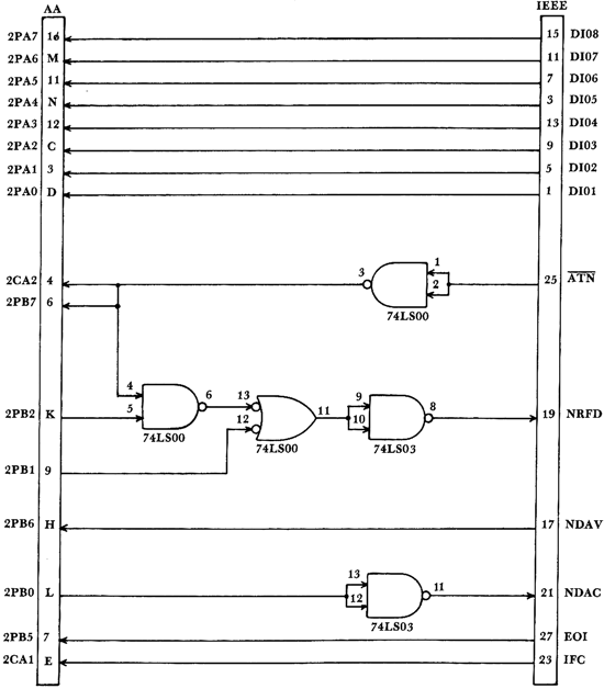
Now we are ready to deal with the hardware requirements for communicating on the IEEE Bus. We will be using 6522 #2 on the SYM for the necessary I/O signals since all of the I/O lines from both ports go to the A-A connector. If necessary, the 6522 supplied as 6522 #3 could be moved to the #2 socket, losing only a few features which aren't needed for this interface. The main hardware requirement concerns a requirement for the delay between ATN going low to the time when NRFD is set low by a device. The IEEE 488 Standard calls for a maximum of 200 nanoseconds for this delay. Though the PET can't operate this fast, it does operate too fast for the SYM to meet this requirement using just software. The solution to obtain the necessary speed is to selectively send the ATN signal back out the NRFD line. The SYM can then assume control of the NRFD line when it is ready. The only other hardware needed are a couple of open-collector gates for the Wire-or requirements of the NRFD and NDAC lines. The circuitry shown in Figure 1 will meet these requirements.
Interface
The main function of the INTERFACE sub-function is to handle the communication sequence for the IEEE Bus. The first decision we must make is how the INTERFACE software will know when a communication sequence has begun, or when the IFC line goes low. Since the IFC signal is supposed to reset the device regardless of its current state, this signal should be tied to an interrupt. For greater flexibility we will tie the ATN line to an interrupt as well. This will allow the SYM to do other things when not being used as an interface.
The use of interrupts now provides a basis for dividing the INTERFACE sub-function into smaller parts. Listing 4 shows my division of the INTERFACE sub-function.
Listing 4
procedure INTERFACE

procedure ATNIRQ begin … end; {handles the IEEE communication}
procedure IFCIRQ begin … end; {resets the interface}

begin {INTERFACE procedure}
   repeat
    if INTERRUPT=TRUE then
       begin
          if IRQ=ATN then ATNIRQ;
          if IRQ=IFC then IFCIRQ
       end
   until 2+2=5 {hopefully repeat forever}
end;
At this point we are almost ready to write the assembly language for the remaining parts of the software. However, ATNIRQ needs one more division. This involves addressing the question of how much intelligence to put in the interface. One answer is to program ATNIRQ in a way that leaves the door open for expansion. This can be done easily using the secondary address to call different interface routines. The division for ATNIRQ is shown in Listing 5. The “case” statement in this listing is a multiway subroutine jump. If SECADDRS is 0 when the “case” statement is executed, the SENDASCII procedure will be executed. For other secondary addresses, the DUMPCHRS procedure will be executed.
Listing 5
procedure ATNIRQ

procedure ATNINIT; begin … end; {get ready for communication}
procedure SENDASCII; begin … end; {input data and print it}
procedure DUMPCHRS; begin … end; {ignore data}

begin {ATNIRQ statements}
CYCLE; {get device address}
if DATA=MLA then
   begin
      ATNINIT;
      CYCLE; {get next byte, possibly a secondary address}
      if ATN=LOW then
         begin
            SECADDRS := DATA;
            CYCLE
         end;
      case SECADDRS of
            0 : SENDASCII;
        1..15 : DUMPCHRS;
      end {case statement}
   end {if statement}
end; {ATNIRQ}
Now we can write the assembly language for INIT, then IFCIRQ, and finally ATNIRQ. Not clearly shown by the preceeding PASCAL programs is how the machine language should actually handle the interrupts. After an interrupt occurs, the first thing the machine language must do is save the register contents. Then it must test to see what interrupt occured. If it was an ATN interrupt, then the current stack pointer must be saved and ATN interrupts disabled before continuing with the rest of the ATNIRQ routine. If the interrupt was an IFC interrupt, the IFCIRQ routine should test to see if the ATNIRQ routine was executing. If it was, the IFCIRQ routine must restore the stack pointer to the value saved by ATNIRQ and reenable the ATN interrupt before restoring the registers and returning to the interrupted program.
The full listing of the assembly language for the interface is given in Listing 6. I've tried to write the assembly language so it can be easily expanded. Just remember that when you put a different routine in SCTABLE, the first data byte will have already been fetched by CYCLE when your routine is entered.
Summary
I've tried to make this article as much an example of interface design as one describing an actual interface. Most of the material presented dealt with needed facts or the steps involved in reaching a solution. I do not wish to imply that designing an interface should proceed from start to finish as easily as this article makes it seem. It is very likely that during your design, you will come upon a piece of new information or see a different approach which would have been highly useful at some previous step. This occured a few times during this design. Sometimes it is necessary or perhaps desireable to return to that previous step and take a different path. However, if you do enough preparation and planning before you begin the design process, you shouldn't have to backup too many times.
Listing 6
                0010 ; IEEE INTERFACE
                0020 ; WITH HARDWARE
                0030 ; VERSION 2.5
                0040 ;
                0050 ; CONSTANTS
                0060 UNLISTEN   .DE $3F
                0070 BS         .DE $08
                0080 UNDLN      .DE $5F
                0090 LF         .DE $0A
                0100 COLON      .DE $3A
                0110 SPACE      .DE $20
                0120 COMMA      .DE $2C
                0130 CR         .DE $0D
                0140 ;
                0150 ; VARIABLES
                0160 COUNT      .DE $E0
                0170 SIGNALS    .DE $E1
                0180 DATA       .DE $E2
                0190 MLA1       .DE $E3
                0200 SEC.ADDRS  .DE $E4
                0210 TEMP       .DE $E5
                0220 LENGTH     .DE $E6
                0230 NL.FLAG    .DE $E7
                0240 SCAN.CNT   .DE $E8
                0250 F.LEN      .DE $E9
                0260 SP.IEEE    .DE $EA
                0270 ;
                0280 ; ADDRESSES
                0290 ACCESS     .DE $8B86
                0300 TOUFL      .DE $A654
                0310 SDBYT      .DE $A651
                0320 TECHO      .DE $A653
                0330 OUTCHR     .DE $8A47
                0340 INCHR      .DE $8A58
                0350 CRLF       .DE $834D
                0360 TOUT       .DE $8AA0
                0370 @2ACR      .DE $A80B
                0380 @2DDRA     .DE $A803
                0390 @2DDRB     .DE $A802
                0400 @2PCR      .DE $A80C
                0410 @2IER      .DE $A80E
                0420 @2IORB     .DE $A800
                0430 @2IORA     .DE $A801
                0440 @2IFR      .DE $A80D
                0450 OUTVEC     .DE $A663
                0460 UIRQVC     .DE $A678
                0470 IND.JMP    .DE $EE
                0480 ;
                0490            .BA $200
0200- 20 86 8B  0500 INIT       JSR ACCESS   ;INITIALIZATION
0203- A9 24     0510            LDA #$24
0205- 85 E3     0520            STA *MLA1    ;MY LISTEN ADDRESS
0207- A9 90     0530 INIT.SYM   LDA #$90
0209- 8D 54 A6  0540            STA TOUFL    ;ENABLE CRT
020C- A9 10     0550            LDA #$10
020E- 8D 51 A6  0560            STA SDBYT    ;SET FOR 1200 BAUD
0211- A9 00     0570            LDA #$00
0213- 8D 53 A6  0580            STA TECHO    ;OUTPUT & NO ECHO
0216- A9 A0     0590            LDA #L,TOUT  ;SET OUTPUT VECTOR
0218- 8D 64 A6  0600            STA OUTVEC+$1021B- A9 8A     0610            LDA #H,TOUT
021D- 8D 65 A6  0620            STA OUTVEC+$2
0220- A9 53     0630            LDA #L,INTERFACE
0222- 8D 78 A6  0640            STA UIRQVC   ;SET USER IRQ VECTOR
0225- A9 02     0650            LDA #H,INTERFACE
0227- 8D 79 A6  0660            STA UIRQVC+$1
022A- A9 02     0670            LDA #$02
022C- 85 E0     0680            STA *COUNT
022E- A9 00     0690 INITPORTS  LDA #$00
0230- 8D 0B A8  0700            STA @2ACR    ; NO LATCHING
0233- 8D 03 A8  0710            STA @2DDRA   ;2PA7-2PA0 ARE INPUTS
0236- A9 07     0720            LDA #$07
0238- 8D 02 A8  0730            STA @2DDRB   ;3PB2-3PB0 ARE OUTPUTS
023B- A9 04     0740            LDA #$04
023D- 8D 0C A8  0750            STA @2PCR    ;INTERRUPTS
0240- 20 47 02  0760            JSR EN.IEEE  ;ENABLE IRQS
0243- 58        0770            CLI
0244- 4C 44 02  0780 IDLE       JMP IDLE     ;WAIT REAL FAST
                0790 ;
                0800 ;
0247- 78        0810 EN.IEEE    SEI
0248- A9 83     0820            LDA #$83     ;ENABLE ATN AND IFC
024A- 8D 0E A8  0830            STA @2IER    ; INTERRUPTS
024D- A9 06     0840            LDA #$06
024F- 8D 00 A8  0850            STA @2IORB   ;NDAC=1, NRFD=ATN
0252- 60        0860            RTS
                0870 ;
                0880 ;
0253- 48        0890 INTERFACE  PHA          ;SAVE REGISTERS
0254- 98        0900            TYA
0255- 48        0910            PHA
0256- 8A        0920            TXA
0257- 48        0930            PHA
0258- AD 0D A8  0940            LDA @2IFR
025B- 10 1D     0950            BPL EXIT.INTF
025D- 29 03     0960 IEEE.IRQ   AND #$03     ;WHICH INTERRUPT?
025F- C9 01     0970            CMP #$01
0261- F0 1D     0980            BEQ ATN.IRQ
0263- C9 02     0990            CMP #$02
0265- F0 03     1000            BEQ IFC.IRQ
0267- 4C 7A 02  1010            JMP EXIT.INTF
026A- AD 01 A8  1020 IFC.IRQ    LDA @2IORA   ;CLEAR INTERRUPT
026D- A9 01     1030            LDA #$01
026F- 2C 0E A8  1040            BIT @2IER    ;IEEE ACTIVE?
0272- D0 06     1050            BNE EXIT.INTF        ;EXIT INTERFACE
0274- A6 EA     1060 IEEE.OFF   LDX *SP.IEEE
0276- 9A        1070            TXS          ;RESTORE STACK POINTER
0277- 20 47 02  1080            JSR EN.IEEE
027A- 68        1090 EXIT.INTF  PLA
027B- AA        1100            TAX
027C- 68        1110            PLA
027D- A8        1120            TAY
027E- 68        1130            PLA
027F- 40        1140            RTI
                1150 ;
                1160 ;
0280- BA        1170 ATN.IRQ    TSX
0281- 8E EA 00  1180            STX SP.IEEE  ;SAVE STACK POINTER
0284- AD 01 A8  1190 ATNINIT    LDA @2IORA   ;CLEAR INTERRUPT
0287- A9 05     1200            LDA #$050289- 8D 00 A8  1210            STA @2IORB   ;SET NDAC=0 NRFD=0
028C- A9 01     1220            LDA #$01
028E- 8D 00 A8  1230            STA @2IORB   ;TURN OFF ATN=NRFD
0291- 8D 0E A8  1240            STA @2IER    ;TURN OFF ATN IRQS
0294- 58        1250            CLI
0295- A9 00     1260            LDA #$00
0297- 85 E4     1270            STA *SEC.ADDRS       ;INIT SEC. ADDRS
0299- 20 EF 02  1280            JSR CYCLE
029C- A5 E2     1290            LDA *DATA
029E- C5 E3     1300            CMP *MLA1
02A0- F0 0C     1310            BEQ DEVICE1  ;BRANCH IF MY ADDRESS
02A2- A9 02     1320 EXIT.IEEE  LDA #$02
02A4- 8D 00 A8  1330            STA @2IORB   ;RELEASE ATN=NRFD
02A7- 2C 00 A8  1340 @15        BIT @2IORB
02AA- 30 FB     1350            BMI @15      ;WAIT FOR ATN=1
02AC- 10 BC     1360            BPL IFC.IRQ  ;BR ALWAYS
                1370 ;
02AE- 20 EF 02  1380 DEVICE1    JSR CYCLE
02B1- 24 E1     1390            BIT *SIGNALS ;SECONDARY ADDRESS?
02B3- 10 09     1400            BPL @3       ;BRANCH IF ATN IS OFF
02B5- A5 E2     1410            LDA *DATA    ;GET SECONDARY ADDRESS
02B7- 29 0F     1420            AND #$0F     ;ALLOW 16 SEC.ADDRS'S
02B9- 85 E4     1430            STA *SEC.ADDRS
02BB- 20 EF 02  1440            JSR CYCLE    ;GET FIRST CHAR.
02BE- A5 E4     1450 @3         LDA *SEC.ADDRS
02C0- 0A        1460            ASL A
02C1- AA        1470            TAX
02C2- BD CF 02  1480            LDA SCTABLE,X        ;FIX POINTER TO
02C5- 85 EE     1490            STA *IND.JMP         ;  SELECTED ROUTINE
02C7- BD D0 02  1500            LDA SCTABLE+$1,X
02CA- 85 EF     1510            STA *IND.JMP+$1
02CC- 6C EE 00  1520            JMP (IND.JMP)
02CF- 37 03     1530 SCTABLE    .SI SENDASCII        ;NORMAL PRINTING
02D1- 47 03     1540            .SI DUMPCHRS
02D3- 47 03     1550            .SI DUMPCHRS
02D5- 47 03     1560            .SI DUMPCHRS
02D7- 47 03     1570            .SI DUMPCHRS
02D9- 47 03     1580            .SI DUMPCHRS
02DB- 47 03     1590            .SI DUMPCHRS
02DD- 47 03     1600            .SI DUMPCHRS
02DF- 47 03     1610            .SI DUMPCHRS
02E1- 47 03     1620            .SI DUMPCHRS
02E3- 47 03     1630            .SI DUMPCHRS
02E5- 47 03     1640            .SI DUMPCHRS
02E7- 47 03     1650            .SI DUMPCHRS
02E9- 47 03     1660            .SI DUMPCHRS
02EB- 47 03     1670            .SI DUMPCHRS
02ED- 47 03     1680            .SI DUMPCHRS
                1690 ;
                1700 ;
02EF- A9 03     1710 CYCLE      LDA #$03
02F1- 8D 00 A8  1720            STA @2IORB   ;NRFD=1 NDAC=0
02F4- 2C 00 A8  1730 @1         BIT @2IORB   ;TEST DAV
02F7- 70 FB     1740            BVS @1       ;BRANCH IF DAV=1
02F9- 6A        1750            ROR A
02FA- 8D 00 A8  1760            STA @2IORB   ;NRFD=0 NDAC=0
02FD- AD 01 A8  1770            LDA @2IORA
0300- 49 FF     1780            EOR #$FF
0302- 85 E2     1790            STA *DATA
0304- AD 00 A8  1800            LDA @2IORB0307- 85 E1     1810            STA *SIGNALS
0309- A9 00     1820            LDA #$00
030B- 8D 00 A8  1830            STA @2IORB   ;NRFD=0 NDAC=1
030E- 2C 00 A8  1840 @2         BIT @2IORB
0311- 50 FB     1850            BVC @2       ;BRANCH IF DAV=0
0313- A9 01     1860            LDA #$01
0315- 8D 00 A8  1870            STA @2IORB   ;NRFD=0 NDAC=0
0318- 60        1880            RTS
0319- 20 47 8A  1890 PRINT      JSR OUTCHR   ;PRINT AND INC. COUNT
031C- E6 E0     1900            INC *COUNT
031E- D0 0C     1910            BNE RETURN
0320- A9 03     1920 ACK        LDA #$03     ;ASCII ETX
0322- 20 47 8A  1930            JSR OUTCHR
0325- 20 58 8A  1940            JSR INCHR    ;WAIT FOR ACK
0328- A9 02     1950            LDA #$02
032A- 85 E0     1960            STA *COUNT
032C- 60        1970 RETURN     RTS
                1980 ;
                1990 ;
032D- A5 E2     2000 @18        LDA *DATA
032F- 29 7F     2010            AND #$7F
0331- 20 19 03  2020            JSR PRINT
0334- 20 EF 02  2030 NEXT       JSR CYCLE
0337- 24 E1     2040 SENDASCII  BIT *SIGNALS
0339- 10 F2     2050            BPL @18      ;BR IF ATN=1
033B- A5 E2     2060            LDA *DATA
033D- C9 3F     2070            CMP #UNLISTEN
033F- D0 F3     2080            BNE NEXT
0341- 4C A2 02  2090            JMP EXIT.IEEE
                2100 	;
                2110 	;
0344- 20 EF 02  2120 NEXT2      JSR CYCLE
0347- 24 E1     2130 DUMPCHRS   BIT *SIGNALS
0349- 10 F9     2140            BPL NEXT2
034B- A5 E2     2150            LDA *DATA
034D- C9 3F     2160            CMP #UNLISTEN
034F- D0 F3     2170            BNE NEXT2
0351- 4C A2 02  2180            JMP EXIT.IEEE
0354- 00        2190            .BY $0
                2200            .EN
SYM to Spinwriter Hardware
Editor's Note: For those of you who don't have issue 1, we're reprinting these two charts. RCL
TABLE 1
| NAME | SET BY | DESCRIPTION |
| DIO1-DIO8 | Talker | Data Input/Output. These lines carry the commands and data. |
| NRFD | Listener | Not Ready for Data. When low, it means the device is not ready to receive data. It is set high when the device is ready. |
| DAV | Talker | Data Valid. When high, it means the data on the data lines is not valid. It is set low once all NRFD goes high and valid data has been placed on the data lines. |
| NDAC | Listener | Not Data Accepted. When low, it means that the data has not been accepted. It is set low once DAV goes low and the data has been latched. |
| ATN | Talker | Attention. Signals that the byte on the DIO lines is a command. |
| EOI | Talker | End Or Identify. Signals that the last data byte is being transferred. |
| IFC | Interface Clear. Resets all devices. |
Figure 1