Nuts and Volts
Gene Zumchak
1700 Niagara Street
Buffalo, N.Y. 14207
In the first N & V discussion, I talked about read/write timing in general, and 6502 timing in particular. Fast TTL chips can be used with the 6502, but so can most of the I/O chips of other processor families, provided all the timing requirements are resolved. Even chips with apparently incompatible timing requirements can usually be accomodated by using tricks like latching the write data, or shortening the write strobe, as discussed in the first column. Let's consider what is required to interface a popular port chip of the 8080 family.
The 8255A port chip has 24 I/O pins, programmable in groups of four or eight bits as inputs and outputs. The ports can be used as simple ports, ports with handshaking (and interrupts) and even as bidirectional buses. The reader might want to dig up a spec sheet to study this versatile chip. The “A” suffix of the part number is important. The original 8255 (without the “A") had long setup and hold time requirements. The 8255A, like newer Intel family chips, has improved timing specs with a 100 ns setup time and 30 ns hold time, completely 6502 compatible.
The low-true read gate of the 8255A, RD, can be the inverted R/W signal which need not (but can be) gated with ø2. The low-true write strobe, WR, is met by the normal 6502 write strobe, which we saw earlier is ø2 NANDed with the inverted R/W line. A high true Reset signal must be provided. Like most peripherals, it has a low-true chip select. Figure 1. shows the connections which satisfy the 8255A's timing requirements.
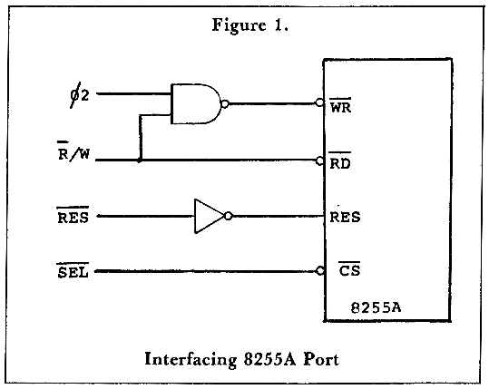
If you have an I/O application requiring more than 16 pins, or you covet some other 8255A feature, there's no electronic reason why you cannot use this chip with your 6502 system. The same can be said of I/O chips from other families. Clearly, all families are designed to be both voltage level and drive compatible with TTL and hence with each other. As we can see, accommodating the read/write timing need not be difficult.
Using Port Chips
The most commonly used family accessory chips are the I/O port chips. However, when simple I/O is required, port chips may not be the best choice. Family chips, including port chips, are not inexpensive. Port chips typically sell in the $8 to $15 range. Since they are MOS devices, their drive capability is usually just one TTL load. They are also vulnerable to static. Since their data bus lines also can only drive a single TTL load, their use is limited to the internal unbuffered data bus around the processor. One could interface them to a buffered bus with bidirectional buffers, but these buffers are expensive and power hungry. MOS port chips, therefore, are most attractive for use in small dedicated controllers, especially where power and parts count are important considerations.
In applications using a buffered bus, where simple I/O is adequate, and where ruggedness and drive capability are important, TTL I/O is more attractive, and usually much cheaper.
TTL Input
To make an input port, we need a set of tri-state® (® trademark National Semiconductor) gates which are gated in unison. A tri-state gate is an electronic switch. When enabled, the output reflects the input (sometimes with inversion). When disabled, the output is high impedance or floating. Thus a large number of tri-state outputs can be bussed together, provided that only one set or device is enabled at one time. RAM chips, ROM chips, and any other devices designed to attach directly to a bidirectional data bus have built in tri-state outputs.
TTL tri-state gates come in quad, hex, and octal configurations. Quad types like the 74LS125 have individual enables for each gate. Hex types like the 8T97, 74LS367, 8097 etc. have four gates with one enable, and two gates with one enable. Although octal gates are the most attractive for eight bit processors, the supply has not kept up with the demand, and hex types are a little easier to come by. Octal types 81LS97 (Nat.) and 74LS244 are not pin compatible.
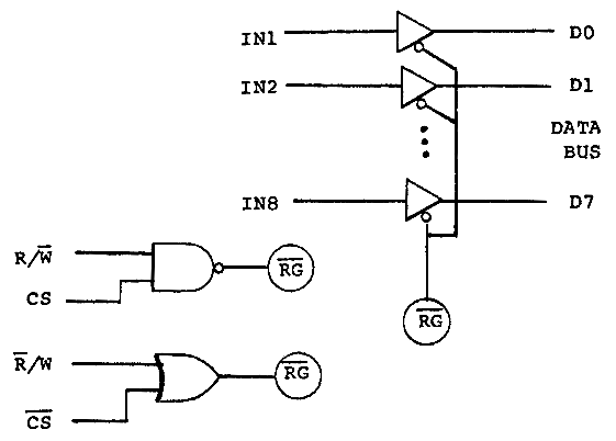
All that's required to use some tri-state gates as an input port is a low-true read gate. This is obtained by ANDing of the R/W line in the read state, and a chip select decoded from the address lines. Figure 2. shows a couple of possibilities, depending upon the polarity of the chip select.
Figure 2. TTL Input Port With Gating
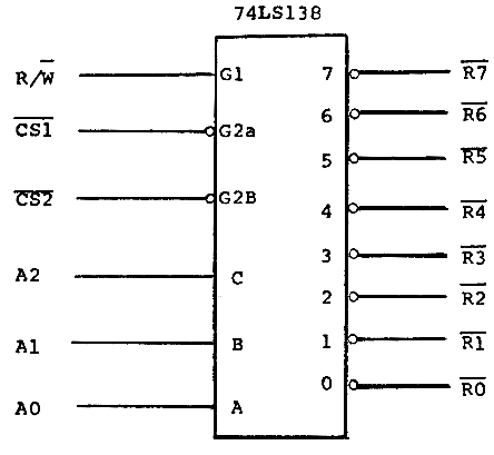
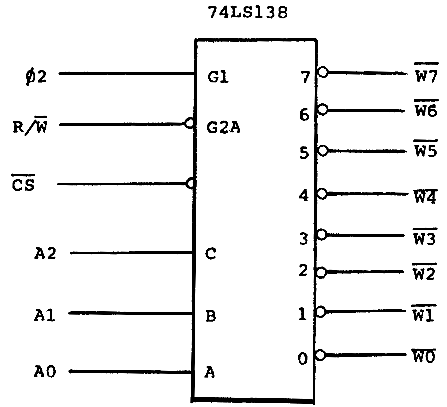
If read gate signals are required for several ports, a single three to eight decoder chip can be used to get eight read gates from a coarser select. The R/W line is used as an enable and is internally gated with all the outputs, as shown in figure 3.
Figure 3 Input Port Read Selects
One nice feature of TTL tri-state gates is that they are always buffers and are meant to drive busses. Low power Schottky devices are more desireable and usually adequate for most applications.
TTL Output
An output bit is a flip-flop which can be written to and from the data bus and whose output is connected to the world. Output bits are usually “D” type flip-flops or latches. In TTL there are several configurations, duals, 74LS74, 74LS109; quads, 74LS75, 74LS175; hex, 74LS174; and octal, 74LS273, 74LS373, 74LS374 and others. Again octal types are sometimes a bit hard to come by.
Output ports need a write strobe generated by ANDing the general purpose write strobe with a select decoded from addresses. Figure 4. shows an output port and the necessary write strobe.
Figure 4. Output Port With Write Strobe
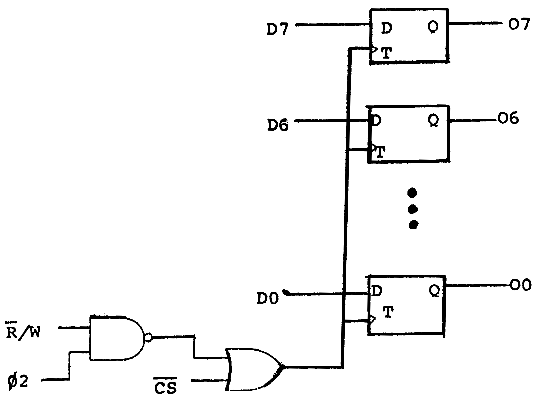
Since TTL devices are very fast, they have setup time requirements of only a few nanoseconds. Therefore the locking edge of the write strobe better come before the data goes away. That is, the ø2 closest to the processor must be used, and not any delayed versions. With a little care, we can use a single decoder chip to generate write strobes for several ports as in Figure 5.
Figure 5. Output Port Write Strobes
From the data sheet for the 74LS138, we see that the delay from the high true enable input (G1) to any output is a maximum of 26 ns (typically 17 ns). This is quite acceptable, provided that we are not using a delayed ø2.
Now if you are building a small dedicated controller, you certainly may not need eight input ports or eight output ports. There's no reason why you cannot use a single 74LS138 to give you gates and strobes for four of each.
Figure 6. Write Strobes and Read Gates
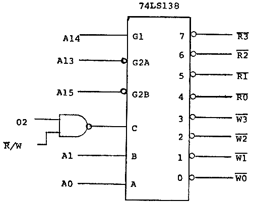
Figure 6 shows a 74LS138 wired to give four read gates and four write strobes. In a dedicated controller, you usually have memory space to burn so that you can afford to waste some. In figure 6. we apply address lines directly to the enables. This puts the ports in an 8K block of memory starting with $4000. The NAND gate generates the general purpose write strobe. It is applied to the “C” input of the decoder. When it is low, a write strobe is generated, when high, a read gate. The maximum delay through the NAND gate is 15 ns, through the decoder, a maximum of 26 ns. Thus ø2 experiences a worst case delay of 41 ns to the trailing edge of the write strobe. This would be acceptable even if there was no data bus buffer delay to compensate it.
Summary
Interfacing I/O to an existing system or a do-it-yourself prototype is not difficult as long as you understand and consider read/write timing. Family chips from any family are useable. Some applications may favor family chips. Others may suggest TTL. The gates and strobes required by TTL I/O are easy to generate.
In the next column I will talk about address decoding and generating selects. Please feel free to write and suggest hardware topics that you would like me to write about.