Programming And Interfacing The Apple, With Experiments
Marvin L. De Jong
Department of Mathematics - Physics
The School Of the Ozarks
Pl. Lookout, MO 65726
Introduction
When the Apple microcomputer is compared with other popular microcomputers, one of its most attractive features is the ease with which it can be interfaced to devices in the outside world. Particularly important in this connection are those eight beautiful card slots in the Apple. The "black box" philosophy of the designers of the TRS-80 leaves much to be desired in scientific, educational, or industrial applications.
In this article we will describe a circuit to be built on a peripheral card that fits in any of the eight card slots in the Apple. The circuit provides the user with one eight-bit input port and one eight-bit output port (with possibilities for expansion). The circuit is built with readily available components, and the output port is also attached to eight LEDs so the user can visualize the state of the bits. The bit values of the input port may be controlled with an eight element DIP switch, or by devices of the user's own choice, such as an A/D converter.
My main reason for designing this circuit was to provide Apple owners with the experiments in my book Programming & Interfacing the 6502, With Experiments. This book was originally based on the KIM-1, SYM-1, and the AIM 65, but with the I/O board described in this article, the book can be used in conjunction with Apple computers. So, if you are interested in learning assembly language programming in conjunction with my book, this I/O board may make the task a little easier. If you are not interested in the book, the I/O board described here will be of interest if you wish to interface your Apple computer to devices like A/D and D/A converters, stepper motors, transmitters, and a variety of other devices.
The Circuit
The circuit diagram is shown in Figure 1. The circuitry on the Apple microcomputer develops a DEVICE SELECT pulse for each of the eight peripheral cards. For card number 0, this pulse occurs whenever addresses $C080 through $C08F appear on the address bus. For card number 1, the corresponding addresses are $C090 through $C09F, and so on for the other card numbers. That is, the device select pulse, DS, is at logic zero for each address in the range $C0N0 through $C0NF, where N = $8 + CN and CN is the card number expressed in hexadecimal. These device select pulses can activate up to 16 I/O ports on each card.
In the circuit shown in Figure 1, the device select pulse (DS) generated by the Apple is combined with the R/W signal generated by the 6502 to produce a signal that activates the 74LS242 bus transceivers in the direction from the Apple data bus to a peripheral card data bus when the R/W line is at logic zero. The lower 74LS32 OR gate and the 74LS04 INVERTER generate this signal. When the R/W line is at logic one during a 6502 READ cycle, the 74LS243 bus transceivers drive the Apple data bus from the peripheral card data bus, provided the DS signal is at logic zero, its active state. Thus, all data bus buffering is handled by the two 74LS243s and it is controlled by the DEVICE SELECT pulse and the R/W line coming from the Apple computer. If you want to reduce the chip count,replace the two 74LS243s with one 74LS245 Octal Bus Transceiver, a 20-pin chip.
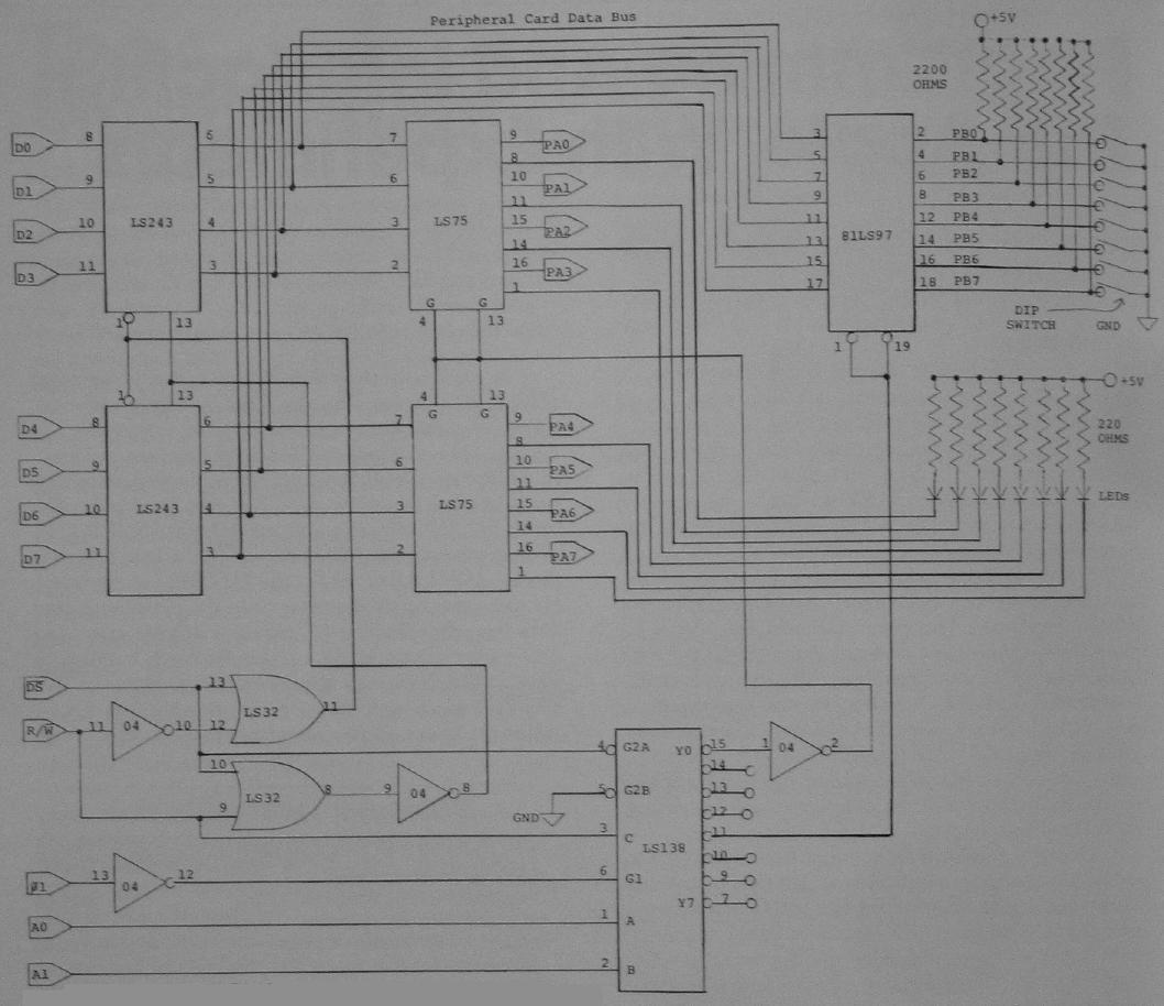
The DS pulse also activates the 74LS138 3-to-8 line decoder that is used to produce up to four WRITE pulses for output ports (Y0 - Y3 pins on the LS138) and four READ pulses for input ports (Y4 - Y7 pins on the LS138). In this application, only one WRITE pulse and one READ pulse are used. You may add more ports. Note that the R/W line is one of the lines decoded by the 74LS138. This idea originated in Gene Zumchak's Nuts and Volts column in Issue 2 of compute II. Thus, the lowest four output lines, Y0 - Y3, on the 74LS138 will be active only on WRITE cycles. The highest four output lines from the 74LS138, namely Y4 - Y7, will be active on READ cycles. In particular, Y0 is active when the last nibble in the address is $0 ($C080, for example) and the 6502 is in a WRITE cycle with the R/W line at logic zero. The Y4 line from the 74LS138 is active during a READ cycle and when the low-order nibble in the address is $4 ($C084, for example).
The two 74LS75 4-bit bistable latches are transparent to the data bus when the G inputs are at logic one. At the conclusion of the WRITE cycle the G inputs are brought to logic zero and the data on the data bus are latched into the Q outputs of the two 74LS75s. These eight pins for the output port we have called PORT A. The Q outputs activate the LEDs in the sense that the LED will glow if the bit value in Port A is one; otherwise they will not glow. If you want to reduce the chip count, replace the 74LS75s with octal latches such as the 74LS363 or 373, but you will have to eliminate the pretty LEDs or find another way to drive them. This completes the description of the output port.
The input port is an 81LS97 octal three-state buffer. It drives the peripheral card data bus when the Y4 line on the 74LS138 is at logic zero. Thus, a LDA $C094 will result in a "read" of the input port if the peripheral card is in slot 1 of the Apple. We have called the input port, PORT B. The bit values of Port A many be controlled manually by the eight switches on the DIP switch package. If the input pin is connected to ground through the switch. a logic zero results; otherwise you get a logic one. If the input port is to be driven by some other circuit, then the pull-up resistors (2200 ohms) are not necessary. A 74LS244 octal buffer may be substituted for the 81LS97, but they are not pin-for-pin compatible. This completes our description of the input port, and the entire circuit.
Construction
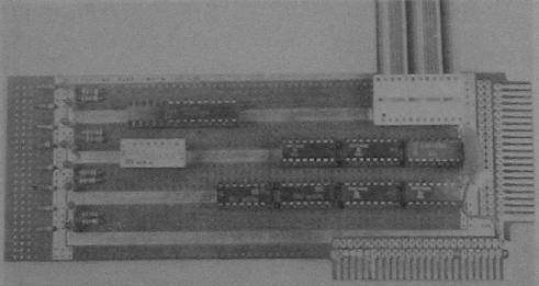
You will need a peripheral card, the integrated circuits, a pin-out diagram for the peripheral card slots (see your Apple manual), soldering equipment, wire-wrap equipment, and several other parts. If you have never wired or built a circuit before, be sure you have someone with experience around who can help you. Two photographs indicate the parts layout that we used. Figure 2 shows the I/O card with the LEDs and switches installed. The pull-up resistors had not yet been wired. Figure 3 shows the I/O card with a ribbon cable DIP jumper connected to a 24 pin socket on the peripheral card. The 24 line cable can handle the I/O port lines and whatever power connections ( + 5V, GND, + 12V, or - 12V) that you might want to steal from the Apple. Another cable alternative would be to use an edge connector on the peripheral card and have the cable exit through one of the slots behind the Apple.
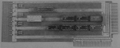
I chose to wire-wrap most of the board, and I purchased my wire-wrap kit (WK-2) and my peripheral card (Vector # 4609) from Jameco Electronics, 1355 Shoreway Road, Belmont, CA 94002. The remainder of the parts are available from a variety of mail-order houses, Jade Computer Products for example.
The best way to start is to make all of the power connections first. These are not shown in Figure 1, but they are completely described in Table 1. Also, although none are shown in the photographs, it is good practice to install one 0.01 microfarad capacitor between +5V and ground for each two integrated circuits before doing the remainder of the wiring. I installed mine later because I did not have any available on the day that I wired the circuit and took the pictures. Next, wire the lines from the edge connector to the appropriate pins on the wire-wrap sockets. These lines all appear to the left of the circuit diagram in Figure 1, and a table of the pin numbers is given in Table 2. Finally, wire the connections between the pins on the sockets. The procedure just described insures that all the soldering is done at an early stage, when you are less likely to burn through several innocent wires while trying to solder another one. Again, if you have had little experience in wiring, find someone to help you lay out the circuit and get started wiring. Most people are anxious to demonstrate their expertise and be helpful.
Testing and Operation
To test the board first turn off the Apple and install the board in one of the slots, say slot 6 in which case the address of the output port is $ C0E0 (decimal 49376) and the address of the input port is $C0E4 (decimal 49380). (Actually, both ports respond to other addresses also, but that will not be of any concern here.) With the card installed and the Apple running in its monitor, write some number to the output port; that is, enter *C0E0:55 RETURN. The LEDs should display $55. Try some other numbers such as $01, $02, $04, $08, $10, $20, $40, and $80 if you wish to try all the LEDs in turn. To test the input port with the monitor simply use it to examine location $C0E4 by entering *C0E4 RETURN. The number you get should correspond to the switch settings. Try each switch in the logic one position in turn to verify that everything is working properly.
To test the I/O card using BASIC you must PEEK at the input port and POKE data to the output port. For example, a statement
10 Y = PEEK(49380)
returns the data at the input port as Y. The statement
20 POKE 49376, Y
will put the contents of Y in the output port, provided Y is not greater than 255. Try running this program:
10Y = PEEK(49380)
20 POKE 49376, Y
30 GO TO 10
It reads the input port and writes that number to the output port. Thus, the LEDs should follow the input switches. In the above test procedure, we are still assuming that the peripheral I/O card is in slot 6. If you select some other slot, then the addresses used above must be modified.
Concluding Remarks
You should be aware that you cannot use read-modify-write assembly language instructions (e.g., INC, DEC, ASL, LSR, etc.) to reference the output port because it does not include an output register. The best way to reference the output port is with STA, STX, or STY instructions. To demonstrate the other instructions, perform all your read-modify-write instructions on some R/W memory location (RAM), then transfer the contents of this location to the output port. For example this program segment demonstrates the ASL instruction.
ASL MEM1 Modify the MEM1 location.
LDA MEM1 Transfer it to the accumulator.
STA PAD Output the data to Port A
If you have any questions, please include a self-addressed stamped envelope, and I will be glad to respond.
|
|