Nuts And Volts
Build Your Own Controllers
Eugene M. Zumchak
Buffalo, NY
The previous article in this series appeared in COMPUTE!, November, 1981, # 18, pg. 160.
In the last installment of this series, I considered what is required to put together a dedicated micro-controller, and covered the CPU, ROM, and RAM. I will continue here with a discussion of simple I/O.
A novice designer might think that there really isn't much to be said about I/O. All one needs to do is to attach the microprocessor's family port chip. In the case of the 6502, this would be the 6522 VIA, an excellent I/O chip. Aside from two programmable ports, the 6522 has two timers, a shift register, and port control bits usable in hand-shaking or as general-purpose interrupt inputs.
For a compact general-purpose controller board, the 6522 is a good choice for minimum I/O. Timer 1, when used in the free-running mode, can provide a crystal time-base for a realtime clock. And including control bits, as many as 20 I/O bits are available. However, when more simple I/O is required, using additional 6522's may not be the best choice. One alternative is to use low-power Schottky TTL. Advantages of using TTL is lower cost, increased ruggedness (not susceptible to static damage), tighter software, and lower power. Surprisingly, a pair of input ports or a pair of output ports realized with LS-TTL requires only about half the current of a 6522.
While some I/O functions can benefit from the fact that the same I/O bits of the 6522 can be programmed as inputs at one moment and as outputs the next, most simple I/O is simply either input or output, and the programmability is more of a non-feature. That being the case, let's see how I/O can be realized with TTL functions, beginning with input functions.
Simple Input
The unit input function is a three-state gate and a suitable gating signal which will be true when a read operation is performed using a specific address. Assume that our input functions will use a coarse address select with base address $2000. (This could be a 1K, a 2K, a 4K, or even an 8K select). A single 74LS138 3-to-8 decoder can be used to further decode this coarse select into eight individual gating signals as shown in Figure 1.
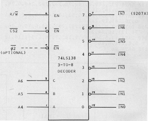
Three address bits, preferably not the lowest, are used to achieve the subdivision into eight selects. The R/W signal is used as an enable so that the eight select outputs can be true only for read operations.
Optionally, the low-true version of the phase-2 clock may be used to restrict gating signals to ø2 time. Now that we have suitable input gating signals we can consider the form of the ports themselves.
Simple input falls into one of two categories. Byte input or bit input. Byte input, of course, is input which is read in and used in a byte form; for example, the output of an parallel ASCII keyboard. While programmable ports are fine for byte inputs, they are less suitable for bit inputs (inputs which are strictly one-bit functions, like the condition of a particular switch).
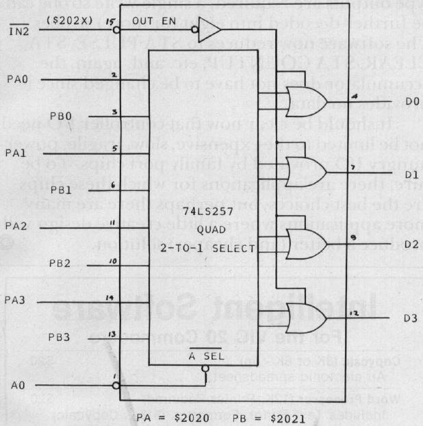
A suitable TTL byte input port would be any of the octal three-state buffer chips. The 74LS244 and 81LS97 are examples, A quick count will show that 20 pins are required for this function. A three-state octal latch like the 74LS373 or 74LS374 can provide a latched byte input port. While a pair of 20-pin chips could be used to provide a pair of 8-bit input ports, a pair of ports can be realized with two 16-pin chips. Figure 2 shows a pair of 4-bit input ports, realized with a single 74LS257 three-state quad 2-to-l select chip. (Two chips will give two 8-bit wide ports.) An address bit, usually A0, is used to select between the two ports. A pair of these chips takes typically 20 mA, much less than a pair of ports from a 6522.
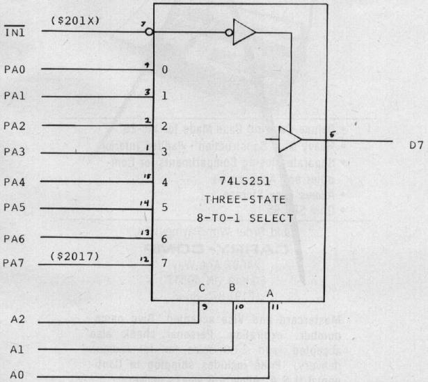
Most designers use byte-style input ports for bit input functions. A particular bit in a port can be isolated for making a decision by loading in the port data, ANDing with an appropriate mask, and branching based on the zero flag. However, an 8-bit input port can be realized with a 16-pin 74LS251, a three-state, 8-to-l select function. The single output bit is brought in on data bit D7. Now any of the eight bits may be individually addressed and tested. Such a bit-addressable port is shown in Figure 3. In particular, any bit can be tested with a BIT instruction to the bit address, followed by a branch based on the sign flag. Thus, input bit tests take only two, not three, instructions, and do not change the A register. Since each individual bit in the port has its own unique address, each bit function in software will have its own unique label, making the software somewhat more readable. That is far superior to calling a byte of eight switches SWITCHES.
Simple Output
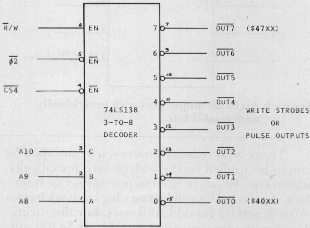
Like simple input, simple output can be bit output and byte output, but also pulse output. As with inputs, the first job is to provide suitable control signals for our output functions. A single 3-to-8 decoder chip can provide eight individual write strobing signals from a coarse address select. (Figure 4.)
In this case, the ø2 clock signal is not optional since write strobing action is accomplished with this signal in 6502 timing. The application of the low-true version of the ø2 delay in the individual outputs and an acceptable amount of write hold-time loss. (See the early Nuts & Volts columns on read/write timing).
Byte style output ports can simply be any of the numerous octal latches in 20-pin packages. While the board space requirement for a pair of such ports is about the same as for a 6522, the power is somewhat less. As with input functions, most designers use byte-style output ports to achieve single bit outputs. The differences are resolved with software. To turn off (or on) a particular bit, without changing other bits in a port, the output port (or status) is loaded, an appropriate AND (or OR) mask used, and the altered data is written to the port. This takes three instructions and eight bytes. However, if a port with individually addressable bits is used, any arbitrary bit can be turned on or off with a single three byte instruction, and without changing the accumulator. The port itself is shown in Figure 5, and uses the not-well-known 74LS259 addressable latch chip. This chip has three address lines to select one of eight output bits. A single data line is used to apply the one or zero to set or clear the selected bit.
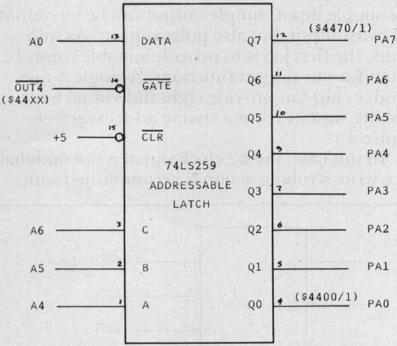
There is no reason, however, why this data bit cannot be applied via the address bits. Specifically, address bit A0 can be used to provide set or reset data. A selected bit will be reset for even addresses (A0 = 0) and set for odd addresses. For the wiring shown in the figure, writing to address $4400 will clear bit zero. Writing to $4451 will set bit five. That is, the least hex digit is either zero or one, and the next-to-least hex digit is used to select one of eight bits. Thus, a STA $4461 will set bit six where the contents of A is totally irrelevant. That is, it is unnecessary to load A (or X or Y) before the write. As with bit addressable inputs, the complementary bit addresses can be given software names like VALVE/ON, VALVE/OFF, BELL/ON, etc. Nothing, software-wise, could be simpler or faster.
Finally, some output functions have the form of one-bit pulses or triggers. These might be external clocks, resets, etc. To achieve a pulse output with a byte-style port requires loading output status, ANDing the selected bit off, writing out the new status, ORing the bit back on, and writing out the new status. This takes a minimum of five instructions and thirteen bytes. A pulsed output can be obtained directly from an unused individual write strobe as shown in Figure 4. If many pulse-type outputs are required, a single write strobe can be further decoded into eight (or more) strobes. The software now reduces to STA PULSE, STA CLEAR, STA COUNTUP, etc. and, again, the accumulator does not have to be changed since it provides no data.
It should be clear now that controller I/O need not be limited to the expensive, slow, fragile, power-hungry I/O provided by family port chips. To be sure, there are applications for which these chips are the best choices, but perhaps there are many more applications where a little creative design will produce a better (and cheaper) solution.