

The
Beginning
It's strange how things really get started in this
world. Here I am, walking down the aisle in my local electronics
supermarket (that's what we have out here in Silicon Valley instead of
Malls...) and a display jumped out at me - 128Kx8 25ns Static RAMS -
$27.00. Wow, that's cheap! I always assumed that cache RAMS that size
would be out of sight, so I have never priced them. Guess the PC guys
use plenty of these things, which drives down the cost... That started
me thinking about what I could do with really fast 128K SRAMs.The other chapter of this story came from a message left on CompuServ by one of the 8-bitters. He was asking Bob Puff, of CSS, about speeding up the 6502 in our machine for better performance. I replied with an idea that Bob should make up a bunch of these high speed 8-bits for all the people interested in them. Bob's answer was for me to send him the second unit I finished - which, at the time, was not a serious proposition. But, considering the SRAM availability and the user interest in this type of upgrade, I have begun to develop a high speed hack in earnest. I won't hold Bob to his participation, but a couple of dozen letters from people waving credit cards might carry some influence with CSS (grin). See, two unrelated incidents got this whole thing started... wheels within wheels...

The
Plan
So, just what have I started here? Just about every
8-bit user at some time or other has wished that his machine ran just a
little faster. Maybe a lot faster. Various techniques have been
developed to save time or increase program speed: turning off the
screen, using machine language in BASIC, re-coding the Operating System
- bunches of hacks. None of them actually address the clock speed of
the Atari. And, for good reason; fooling around with the clock is very
difficult to do in your attic.Sure, if we were Intel or Motorola, we could just whip up a bunch of 90mhz chips and slap them on a multi-layer printed circuit board with transmission line quality ground planes and the latest SMD technology. After a careful search, I failed to find those kinds of tools in my attic.
Anyway, increasing the clock speed of the 6502 in your 8-bit would do wonders for your system's performance without requiring new software or any of those nasty compatability problems.
The
Result
The current clock speed is 1.79 mhz, which allows
approximately 30,000 6502 clock cycles per video frame. The ANTIC chip
in your 8-bit "steals" 10,000 clock cycles in every frame to generate
his video, so the 6502 is left with 20,000 to do computing things with.
This means that you can turn off ANTIC and get back almost 10,000
cycles per frame (but you now have a blank screen... ).What I am going to discuss is a hack that runs at 14.36 mhz; eight times the clock speed of your 6502. That's 240,000 clock cycles per frame. With ANTIC taking his 10,000 cycles, you will have 230,000 left for your favorite software, 10 times what you have now! Sound good? Sure it does!
Wish we could do something like that, but we can't. What we can explore is a useful modification that will give you 210,000 more cycles per frame without a lot of changes inside your machine.
The
Issues
The issues surrounding a project to increase your
clock speed deal mostly with the buss and the interface to the other
chips in your computer.Let's look at the buss first. The printed circuit board (PCB) in your Atari is designed to run at 1.79 mhz. I took a 600XL PCB (these 600XL boards are great to experiment with) and pulled all the chips out of it with the exception of the OS ROM and the CPU. I was going to see how the buss would act at higher speeds, starting with a 3.58 mhz clock. Looked pretty good. Add another chip. Not so good. Add a third chip and you no longer have a viable circuit. The nice little square signals get all squished and rounded.
This is the normal result when you add more chips to an inadequate buss, the signal quality goes to heck. No way to run the existing buss at higher speeds, regardless of the quality of chips used.
You might think to run the board at just a 50% increase (2.68 mhz) instead of a 100% increase, but any clock change must be a 2x multiple of the original frequency or you won't be able to hook it up to your monitor. This is why the PAL computers need different clock speeds; their monitors run at a different rate than ours.
No question then. Anything running at high speed has to be on it's own PCB, one designed to run over 1.79 mhz. This means that we can't use the memory, ROMs, or the logic chips already in our computers for the new CPU unless we kick the clock back down to 1.79 mhz.
The other issue is the limited clock speed of the custom chips in our 8-bits. Of major importance are the ANTIC/GTIA pair and the POKEY chip. These are chips designed specifically for the Atari computers. We can get much, much faster logic chips, memory and even make a faster 6502, but we can't make a 14.36 mhz ANTIC. Here again, when we talk to these chips, we have to kick back down to 1.79 mhz - even if we build a new PCB that runs at 14 mhz.
So, we need to do two things: build a separate PCB and put all the high speed electronics on the new board. This is not going to be easy - maybe that's why none have been produced yet. Let's continue.
The
Method
The basic principle in cranking up the clock is to
share system memory between a new 65816 CPU and the rest of your Atari.Take a look at the Aux Processor Clock Timing figure. The top line represents the 65816 CPU clock synchronized with the bottom line, the system clock. There are eight CPU cycles, designated 0-7, for each system cycle. In the course of any cycle, the memory address is placed on the buss for the full cycle. This gives the memory time to select the cells that hold the data. At the end of the cycle, the data is either read from the buss if reading, or written into the memory cell if writing.
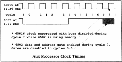
The key point is that all data transfers really take place at the end of the cycle. Everything up to that point is just setting up addresses.
Now, if we use really fast memory, we can get in and out of memory many times during the 6502 cycle. The normal 8-bit memory takes 200ns to set up addresses out of a cycle of 280ns (it can only be active on the last half of the cycle).
Works fine at 1.79 mhz. The cache SRAM I saw runs at 25ns - out of a 35 ns cycle. Plenty of time! The 65816 can go to memory 7 times while the 6502 is setting up addresses. On the 8th cycle, we gate the 6502 onto the buss and let him use memory for one cycle.
Everybody is happy. The 6502 has no idea that he is sharing his memory! Now, one more point. Notice that I talk about the 6502 and the 65816? Aren't we going to replace the 6502? Well....
You can replace the 6502, but it isn't easy. If you make the 65816 drive the other chips (ANTIC, POKEY, etc.), you have to include circuits to get everybody in sync.
Look at the timing chart. Suppose you are going to STA some data in ANTIC in cycle 3. You not only have to stretch out the clock to 1.79 mhz, but you have to wait until the longer clock is in sync with the 6502 clock. You need to check for this condition (slowing down and syncing) on every 65816 clock cycle. This takes time... And we only have about 20ns to do this checking (along with our normal "where am I" logic stuff).
It could be done, but I think it is beyond the scope of my attic. Instead, why not just use an auxillary 65816 processor and leave the 6502 alone?
The 8-bit can just tool along like nothing is happening. The 6502 will do all the interrupts, run ANTIC, POKEY and all those guys. In fact, without a specific intent, the computer runs exactly the way it ran before the upgrade. This insures comparability with all the existing software.
Unfortunately, it also means that without a change, the software will also run just as slowly as before. This is not as bad as it seems. What purpose would there be in running Pole Position at light speed?
We can make modifications to things like the OS to speed it up independently of the software, as well as BASIC and other tools. And, of course, we can write new routines that run in the '816 very quickly.
The
Details
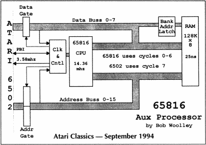
Ok, how would this work? Take a look at the Aux
Processor diagram. One advantage in using a second processor is that
the only signal needed that is not on the PBI buss is the 3.58 mhz
clock for the 6502.This means that anyone who might want to produce this type of upgrade can plug it into the PBI instead of requiring six zillion wires inside the computer. Sadly, the computer will need to be opened to add the one 3.58 mhz clock line. Otherwise, the 6502 buss is connected to data and address gates that are active during clock cycle 7.
Internal RAM is disabled entirely (uh-oh, no RAMBO?). See the block marked Bank Addr Latch? The SRAM is 128K. This latch sets which half of the bank is selected during access. It is set by the 65816 on each '816 cycle, giving the '816 a 128K linear address space. Of this space, 64K "belongs" to the 6502 for his use. The other 64K is where the '816 routines (that you write) will be executed.
For example, you want to move a block of data from $4000 to $6000 in the 6502. You could have a routine up in $012000 in the 65816 memory that does just this. Just point the '816 at the addresses and "tell" him to do it. Nothing takes up 6502 memory and the 6502 just waits while the 65816 runs the routine at super high speed in his own memory bank.
Even the Zero Page and Stack for the '816 are in the $01000 bank! Any interrupts that occur during the routine will be handled concurrently by the 6502 while the '816 keeps on movin'.
One application that also comes to mind in using the two banks is a hard switch. Since the 6502 can use either bank for it's memory, an external switch can be used to "flip" the 6502 into the other bank. If this is done in conjunction with an NMI, the entire memory space as well as the PC will be preserved in the SRAM. Sort of an instantaneous snapshot that you can return to with an RTI and another bank switch.
This would make a super development system! You could bank out of the 6502, look at everything in the system and return when you were finished without changing a single byte.
There are a few things missing in that last explanation. Like, just how do we tell the 65816 to do something for us? How do we get the code into the '816 address space?
The 65816 is inactive after reset while the 6502 goes thru his normal bootup. At this point, the 6502 is using one of the two 64K banks in the SRAM. Doesn't matter here which one, since the '816 is not cycling.
The normal configuration should be for the 6502 to use $00000 thru $00FFFF (bank 0), but reset does not affect the 6502 bank register, so the 6502 could be in either bank after a reset. From power on we would want to start the 6502 in bank 1 so we can load the 65816 code (we need to designate a block of control addresses to control banking - let's pick $D600).
When we first boot the 6502, store $01 in the bank register at $D600. If the system goes out to lunch, then we must have been in bank 0. Just hit reset and re-boot. We are now in bank 1. From here, we need to load the SRAM at $01xxxx with the reset code for the '816.
To the 6502, it will mean setting the OS space as RAM and storing the '816 code up there. Now, when we start the '816, he will see code up in $01xxxx that he will use to manage your 6502 requests. The 6502 can then store $00 into $D600 and return to bank 0 after he starts the '816. Your 65816 code will stay out of bank 0 until the 6502 asks for help.
To execute a 65816 routine, the 6502 can use $D7xx addresses (neither $D6xx nor $D7xx are normally active in the 8-bit, so no other program will try to use it). The '816 can watch location $D700, as an example. If it is $00, then do nothing. The 6502 might then store $04 in $D700, meaning: 4 parameters are now present for execution, the first is the address of your 65816 routine. The '816, when he sees this value would invert the $04 to $FB, indicating he accepted the request and is busy. When the '816 finishes his task, he will zero the flag at $D700, indicating he is not busy.
The 6502 can therefore go off and do whatever he wants without waiting for the '816 to signal completion. If the 6502 wants the '816 to run more routines, he can just check $D700 for $00.
Seems fairly simple, doesn't it? It can be very powerful, though. Put the math chip routines from the OS in the '816 where they will execute at high speed and a lot of software will get supercharged.
The
End
Of The Beginning
Sound like something you would be interested in?
I've been going here for quite a while now. It's time for you users out
there to say your piece. Sometimes writing an article like this gives
the author the impression that he's talking to himself. Take a few
minutes and send you opinions to AC. Tell us what you would like to see
this project grow into.Of The Beginning
I'd hate to think that only two of these will ever get built, one for me and one for Bob Puff, just because they don't meet your needs. I don't want to hear about Pentium projects and 64 megs of memory - try to stay within the scope of the design, OK?
See you next issue!
Bob
* These projects tend to remain unfinished. Proceed at your own risk.