
Atari Zucchini.
by Lee S. Brilliant, M.D.
If you've ever had a garden, you probably grew zucchini-and you know how hard it is to get rid of the stuff! You never plant more than one plant. Even then, it will produce more green stuff than the U.S. mint. When you're ankle deep in it, you try to unload some of the veggies on the unsuspecting neighbors. So you make a trip to your neighbor's house with a twenty-pound beauty-only to find your neighbor waiting at his door with a zucchini of his own for you. Soon you're innundated with zucchini; if only there was another use for this prolific vegetable.
In 1979, Atari began selling its first home computer, the 400. Shortly thereafter, its bigger brother the 800 (remember when they came with a whole 16K?) appeared. Then they produced the ill-fated 1200XL, followed by the 600XL/800XLs. Finally, they introduced the 65XE and 130XE. What does that mean? It means most Atari users have upgraded. I paid $399 for my 800, $199 for my 800XL, and today you can get a 130XE for $129. But what happens to all those old 400, 800, 600XL, 800XL, 1200XL computers, and all the RAM expanders that were produced for them?
Sure, a lot are in the hands of users right this minute. Others are sitting around gathering dust. You can buy them used for peanuts (a legume, not a vegetable). Of course, selling them is like trying to give away zucchini-everyone has one by now.
What
makes a peripheral.
In writing this series, I've always tried to
illustrate theory with simple construction projects. When working on
the serial port sections, I was trying to devise an easy-to-build
peripheral that could communicate with the Atari. As I researched, I
found it was technically much too difficult for the average reader.
Then I saw an article in an electronics magazine on how to build a
printer buffer. I never built it, because it would have cost as much to
build as to buy one already put together. The memory chips alone cost
$32, and there were custom ROM chips you had to buy from the author-for
a tidy profit.Now wait a minute! ROM chips in a memory buffer? It turns out that a buffer is nothing more than a small, dedicated microcomputer. This one used a Z-80 processor, 64K of RAM and a custom ROM, some address decoding, a serial input port, an 8-bit parallel output port, and so on. Add a keyboard, a video circuit and some sound, and you would have a full-fledged computer. I was surprised to find out the venerable 810 disk drive has a 6507 heart-that's a close cousin to the 6502-running the show in your Atari.
Putting all this together, I found out that one Atari could be used to communicate with another through the serial port. It only takes some modified cables and some software. If you're willing to follow this somewhat difficult series of three articles, you'll understand how the Atari communicates through the serial ports and how interrupts are used; then you can build your own functional printer interface/buffer from a surplus 400/800 computer-for around $40.
What shall we call this creation? Why, the Atari Zucchini, what else!
Project
outline.
A thorough description of how the Atari communicates
serially would take several chapters in a book, but I'll try to
condense it into three articles. First, we'll consider the hardware,
then the Serial I/O (SIO), then finally, how to grow your Zucchini.Let's start with the 6520 PIA and POKEY, and see how they handle the interrupt system-and how this relates to SIO. Next month, we'll check out the operating system, to see how serial I/O is accomplished. Our third episode will show you the software and hardware involved in turning an Atari into a printer interface/buffer.
The 6502 CPU has two pins which, when set to 0, will cause it to stop operation and execute a special program called an "interrupt." The two pins are labeled NMI and IRQ, which stand for "Non-Maskable Interrupt" and "Interrupt ReQuest," respectively. When these pins are set, the processor will finish its current instruction, save its place in the current program onto the stack, and jump to the INTERRUPT PROCESSOR program. The processor will determine the source of the interrupt request and be routed to the specific interrupt handler for that source.
For example, pressing a key causes an IRQ interrupt, so the processor determines that the keyboard is requesting service, and then routes to the keyboard handler. The handler should end in a RTI instruction (NMI) or PLA,RTI (IRQ). The locations of the processors are stored in the last few bytes of memory; in this case, the Operating System (OS) ROM. The IRQ vector is at $FFFE and $FFFF, while the NMI vector is at $FFFA and $FFFB. NMI and IRQ interrupts differ in two major respects: (1) the CPU must respond to a signal on the NMI pin, but can be programmed to ignore one on the IRQ pin; and (2) IRQ interrupts affect the processor registers, while NMIs do not. IRQs set the I bit of the Process Status Register, which can be programmed to ignore the interrupt-that is to say, the interrupt can be "masked." To do this, you use the machine SEI and CLI commands. The CPU cannot be programmed to ignore an NMI, hence the "Non-Maskable" appellation.
The only NMIs in Atari are Display List, Vertical Blank and Reset, so these are generated by ANTIC. The interrupt processors are in ROM and cannot be altered, but the IRQ handler first travels through a RAM location (called a "vector") which can be changed and thus rerouted to a processor of your own design. The NMI processor does not have a vector in RAM which can be changed, so no modifications to the NMI handler are possible. (This does not apply to an XL or XE, where ROM can be replaced by RAM and the OS moved. There will be an addendum on this at end of third article.)
While an NMI is not maskable at the CPU level, it is maskable at the ANTIC level. This is done through a special pair of registers residing in ANTIC. NMIST (NMI STatus) is a Read-Only register at location 54287 ($D40F). Whenever an NMI is requested by ANTIC, this register will show which kind of interrupt is wanted. So if ANTIC wants to generate a DLI (called by adding a 128 to any line command in the Display List), it sets Bit 7 of NMIST.
| BIT 7 | BIT 6 | BIT 5 | 4,3,2,1,0 |
| Display List Interrupt |
Vertical
Blank Interrupt |
Reset | Unused |
Before ANTIC will drop its NMI line for a requesting interrupt, it checks the Write-Only register NMIEN ($D40E NMI ENable), to see if your program will allow this interrupt to occur. To ENABLE DLIs or VBIs, you must write a 1 to the proper bit of NMIEN. ANTIC then checks NMIEN against NMIST before allowing the NMI request to be passed along to the CPU. Since NMIEN is Write Only, you may want to keep a shadow register in RAM which contains NMIEN's current value.
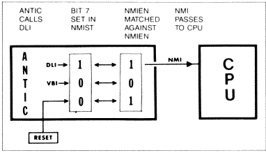
Figure 1. - Outline of interrupt
process.
The CPU will finish its current command, read locations $FFFA and FFFB, and jump to the address stored in these bytes. The address held there contains the location in memory of the NMI processor. The processor reads NMIST and routes the program flow to either the VBLANK routine or the DLI program, or initiates the Reset chain. DLI and VBI programs next route through a vector address located in RAM, then back to the handler in ROM. The handlers can be intercepted at these vectors so you can modify or replace them, but the Reset chain has no vectoring until you reach the point where DOS is called for initialization. Bit 5 of NMIEN is always set so you cannot mask a RESET.
IRQ interrupts work the same way. POKEY contains two registers called IRQST (IRQ STatus) at address $D20E, and IRQEN (IRQ ENable), also at $D20E, that work just like NMIST and NMIEN, in that an IRQ is actually generated - but only if the bits match. If the proper bit in IRQEN was not set, then POKEY will not create the IRQ. The bit assignment of IRQST are as follows:
| Bit | Decimal Function |
| 7 6 5 4 3 2 1 0 |
128
...................................... BREAK key enable 64 ...................... KEYBOARD interrupt enable 32 .................... Serial data input ready (VSERIN) 16 .............. Serial data output request (VSEROR) 8 ............. Serial data output complete (VSEROC) 4 ....................... POKEY timer 4 interrupt enable 2 ................................................ POKEY timer 2 1 ................................................ POKEY timer 1 |
So, to disable the BREAK key, write a 0 to bit 7 in IRQEN, plus its shadow. When you press the BREAK key, no interrupt is generated, because it's blocked at the POKEY level.
All of these interrupts (except the BREAK key in the 400/800) have RAM vectors which can be altered to point to your own routines. The TIMER vectors point to a dummy ROM routine, consisting of PLA and RTI, while the BREAK key has a routine to set the BREAK KEY FLAG at 17 ($11).
Note that three of the POKEY interrupts are involved with serial I/O. We'll look at these later. The timers are described in the Atari tech manuals and are not used in Zucchini. However, we will disable the BREAK key and alter the keyboard interrupt. IRQEN is a Write-Only register; once written to, you cannot retrieve that data. That's why there's a shadow register at location 16, called POKMSK (POKey MaSK), which must always be changed whenever IRQEN is varied, to keep track of which interrupts are enabled.
Once the IRQ is validated and the request generated, the main processor JMPs to the interrupt processor, which tests the various bits of IRQST-to determine the interrupt actually calling-then does a JSR to the appropriate interrupt routine. Since all IRQs have a RAM vector which can be changed, you can reroute any IRQ to your own routine in RAM, instead of to the built-in one in ROM. Try this program:
10
DATA 238,198,2,238,298,2,76
20 FOR S=1536 TO 1542:READ D:POKE S,D:
NEXT S
30 POKE 1543,PEEK(520):POKE 1544,PEEK(
521)
40 POKE 520,0:POKE 521,6
20 FOR S=1536 TO 1542:READ D:POKE S,D:
NEXT S
30 POKE 1543,PEEK(520):POKE 1544,PEEK(
521)
40 POKE 520,0:POKE 521,6
This program intercepts the keyboard vector to cause a change of screen color whenever a key is pressed, then goes on to the normal key process. The vector for the keyboard handler is in locations 520/521, but, if you use the same program with the global IRQ handler vector at 534/535, then the screen will change with any interrupt-such as serial I/O. You can use this simple system to create displays that change during I/O; this will keep you occupied during long loads. You can disable all POKEY interrupts with POKE 53774,0:POKE 16,0. You'll need the RESET key to recover.
By now, you should be familiar with the I/O functions and how to program the ports for input or output. In addition to the port pins, there are four other IRQs associated with the 6520 PIA, besides the POKEY IRQs. While the port pins go to the joystick plugs, there are four additional lines which go to the serial port. These four pins can generate interrupt requests directly, bypassing POKEY, and two of them are programmable for output.
PORTA has two interrupts, PA1 and PA2. Similarly, PORTB has PB1 and PB2. The functions of these interrupt bits are controlled by PACTL (Port A ConTroL) and PBCTL according to this pattern:
| PACTL BITS | |||||||
| 7 |
6 |
5 |
4 |
3 |
2 |
1 |
0 |
| PA1 status |
PA2 status |
PA2
Interrupt control |
Data direct register |
PA1
interrupt control |
|||
The same pattern applies to PBCTL($D303). You should recognize that bit 2 is the one you alter when reprogramming the joystick pins.
When the interrupt control bits are set for input and enabled, an IRQ is generated whenever a trigger pulse comes in over an interrupt line. The last 2 bits of the port control register show which interrupt line was triggered. The Port Control bit patterns to control the interrupts are as follows:
| PA1/PB1 | |
| BIT 1 | BIT 0 |
| 0=Responds
to -transition 1=Responds to + transition |
0=Disable
interrupt 1=Enable interrupt |
| PA2/PB2 | ||
| BIT
5 0=Interrupt from PA2/PB2 1=Output to PA2/PB2 |
BIT
4 0=Responds to - transition 1=Responds to + transition 0=* 1=Direct output |
BIT
3 0=Disable 1=Enable * 0=Logic 0 1=Logic 1 |
| * =Too complex and not pertinent. | ||
Interrupt
controls.
PB1 is connected to Pin 13 on the serial plug. If
you trigger this line, an IRQ is created and bit 7 of PBCTL is set to
1. These bits are tested by the IRQ Processor, which then vectors to
the interrupt routine. The flag bits are reset by a READ operation to
the control registers. Note that the OS Interrupt Processor does not
recognize PA2/PB2 interrupts, only PA1 and PB1 because Atari only uses
these lines for output. You would have to create your own handler for
these.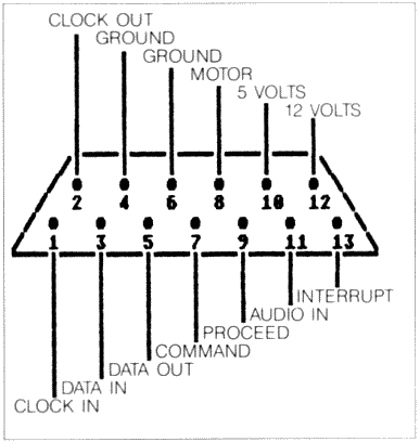
Figure 2. - Serial port, computer side.
Serial
Plug.
The PA2 and PB2 interrupts can be reprogrammed as
outputs. In the Atari, PA2 controls the cassette recorder, while PB2 is
involved in SIO. PBCTL and PACTL usually hold the number 60, which sets
bits 2-5 to 1 or enables PAZ/PB2 for output and sets the lines high.
PA1 and PB1 are similarly available on the serial bus, have vectors in
RAM from $0202 to $0205, are not controlled by IRQEN, and are unused as
far as I know. If you have the fortitude, you can try the following
program to demonstrate.10
DATA 238,198,2,238,198,2,104,64
20 FOR S=0 TO 7:READ D:POKE 1536+S,D:N
EXT S
30 POKE 516,0:517,0
40 POKE 54019,61
20 FOR S=0 TO 7:READ D:POKE 1536+S,D:N
EXT S
30 POKE 516,0:517,0
40 POKE 54019,61
Line 40 sets PBCTL for transition and enables PB1, while Line 30 steals the PB1 interrupt vector to point to our routine. Now, remove the serial plug and attach a small insulated alligator clip to pin 13 of the port and another to pin 4 or 6. Touching the free ends together causes the screen to change color. Note that interrupt lines respond only to transitions in logic state, not the logic state itself. POKEing PBCTL with 63 causes the screen to change colors when the connection between the clip leads is opened.
Standard 6520 design puts ports and interrupts together to create two 8-bit I/O ports, each with 8 data bits, a strobe and a busy line. In the Commodore, all these lines are available in the user's port. In the Atari, the interrupt lines are available only on the serial data port, while the data lines are at the joysticks. (Apple doesn't even have a PIA!) We can use them together to create our own devices. All interrupt routines must end in PLA, RTI instructions, or the computer will get lost.
So, what can you do with this power? Consider this: you could run a BBS, but your burglar alarm might interrupt the BBS to let your Atari telephone a message to the police via your speech synthesizer. What about concurrent processing or multitasking?
The big advantage of interrupts is that they allow for occasional processor use only when needed. For example, there's a portion of the operating system that reads the joysticks and triggers, then transfers this information to the shadow registers every VBlank, so that your program can continually watch the shadows for any changes. Now, if you want to play music while juggling joysticks, you have to squeeze the joystick checks into your music loops. You could use a VBI to load music and free up your program to read the joysticks only.
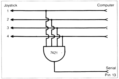
Figure 3. - Joystick port inputs.
Many programs use VBI routines to update player positions or make other changes, leaving main program lines to do other things. A better way, however, is to use an interrupt like the keyboard does. The OS doesn't spend its time scanning the keyboard, waiting for a keypress. Instead, POKEY scans the keyboard and signals the CPU to process a keypress via an IRQ. So a slightly different approach to joystick port inputs might look like Figure 3.
With the circuit in Figure 4, whenever any switch is pressed, it will generate an IRQ which can read the joystick and determine which actions to take. You could use this idea with an encoder chip to give multiple inputs:
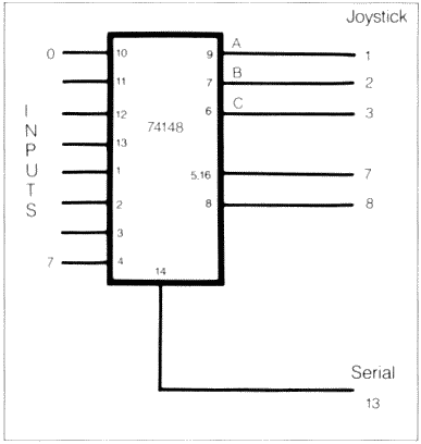
Figure 4. - Another approach using an encoder chip.
For the technically minded, this circuit works as follows:
When all of the input and reference lines to the comparator are equal, the equals output is high.
If any of the input lines changes state, the equals line drops, generating a pulse for the interrupt line. The resistor/capacitor combinations create a short time delay between a change of the input and the catch-up of the reference lead.
When the reference lead again equals the input, the equals line returns to high.
Whenever the mouse moves, it now generates an interrupt, so the CPU can read the position of the mouse. Remember the 74LS14 will "invert" the value of the photo transistor.
The ultimate extension of this interrupt/joystick combination would be a remote keyboard run through the joysticks. Perhaps another article...
Computer designers often face a problem deciding if something is better done in the hardware or software. Such a dilemma is illustrated by "Mouser" (ANALOG Computing issue 40). The author had to use several software manipulations to obtain a high sample rate of the joystick ports to watch Mouser's position. While it simplifies the hardware, this consumes a lot of processor overhead and makes integration with other programs difficult because of the extensive DLI and VBI routines.
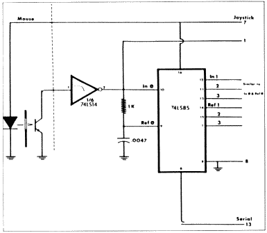
Figure 5. - Mouser circuit.
This simple circuit in Figure 5 generates a short pulse whenever the logic state of Mouser's sensors changes. This pulse in turn triggers the interrupt line on the serial port, so your interrupt routines could read the mouse position on the joystick port. No VBI or DLI changes are needed, making it easier to integrate into other software.
Next month we'll delve further into POKEY, the operating system, and how serial I/O is accomplished. Until then, keep on plugging-or is that unplugging? Oh, and don't eat any used zucchini!