PARALLEL BUS REVEALED
Part III: Building the serial i/o boardby EARL RICE
In Part Three of this important four part series, we're ready to
build a serial I/O board to take advantage of the 100,000 bytes per second
data transfer speed of the Parallel Bus Interface on the Atari XL computers.
In the first two parts of this series, we learned the basic concepts of the Atari Parallel Bus Interface. This month, we'll start the actual design of a serial I/O device for the PBI. We'll choose our devices and set up the logic to allow the computer to talk to the 2K ROM or the USART that we'll use for I/O. Next month, we'll design address decoders and put software into the ROM to make things work.
Figure 1 is a block diagram of the devices we'll work
with this month. Notice that the signals coming into the select logic are
the same ones we invented on our block diagram last month. The exception
is RST which comes directly from the PBI connector. The 2K ROM is a 2716,
available from almost any surplus house. Be sure to get the 350ns version
or it will be too slow for your computer.
The USART and Baud Rate Generator are from Radio Shack. See
the parts list for catalog numbers. I picked this USART because it is readily
available. It is also simple to design with because it has only four registers
to deal with, and all are brought out to IC pins. That means we can hard-wire
some functions and save writing unnecessary software. Next month we'll
explain how you can make the circuit more programmable if you prefer to.
For this example, however, we'll hard-wire the control register
to give us 300 baud, 7 data bits, no stop bits and no parity. Figure
3 is a description of USART pin functions and has the information you
need to change the data format. Figure 4 and its associated table
show how to change baud rate. Note that the Baud Rate Generator has to
run at 16 times the baud rate you want from the USART.
The select logic bears some discussion. Because PBI timing requirements
are tight, we need to use fast logic chips to be sure things work. To make
matters worse, the PBI can electrically drive only one low power TTL load.
When we decode addresses, we'll either need to tie two gate inputs to some
lines and overload them, or put a low power buffer on the line and add
an extra gate delay to our circuit. Neither alternative is very attractive.
Fortunately, there is a logic family available that combines
the loading characteristics of CMOS with the speed of Schottky TTL. This
combination of high speed with virtually no DC load on the PBI lines is
just what we are looking for. The logic family is the 74HCTXX series. These
are the parts to use here. They are exactly function and pin compatible
with TTL.
Be sure to get 74HCT parts and not 74HC parts. The HCT series
is a little scarce on the hobby market, but they are available. I got mine
at JDR Microdevices in San Jose, California.
Figure 2 is a schematic diagram of our serial I/O device. Notice
that the address lines to the 2716 ROM are left off. This is to avoid clutter.
We'll put them in next month when we do address decoding. IC's 4 and 5,
the NAND and NOR gates, are the select logic.
The 2K ROM is selected when the signal from the DEVICE ENABLE
LATCH is LOW AND D8XX-DFXX is LOW Follow the path through the two NOR gates.
You'll notice that the second one is used as an inverter. LOWs at both
pins 4 and 6 produce a LOW at pin 13, giving CHIP SELECT (CS) to the ROM.
This doesn't allow the ROM to be read, however, because its
POWER DOWN (PD) line has to be brought LOW to enable the ROM outputs. The
R/W signal does that every READ cycle. When it brings pin 9 of IC-4 HI,
pin 10 goes LOW, enabling the ROM outputs. When both CS and PD are LOW,
the ROM is on the bus.
We use R/W for the PD signal because its state is set at the
beginning of the 6502 machine cycle, and the PD input takes about 250ns
to work. If we waited for address decoding, a slow ROM might not come on
quickly enough. CS operates in less than 3Ons, so there's plenty of time
available to wait for decoding and device enable to happen.
The USART is set up to operate as a single read or write register.
Any address from $D100 to $D1FF will enable the USART This wouldn't do
at all if we wanted to program its control functions or read its status
register. But we've hard-wired those functions for our example, so it really
doesn't matter. Besides, it saves parts cost.
Next month we'll deal with embellishments. For now, writing
to any address in the $D1XX range puts a character into the transmit register
and the USART will send it. Reading any address in that range reads the
last character received by the USART The DSl-DS8 pins go to the transmit
register, and the RD1-RD8 pins go to the receive register. We've wired
them together and connected them to the data bus so the computer can write
and read USART data.
When the signal from the DEVICE ENABLE LATCH is LOW at pin 3
of IC-4 AND the $D1XX signal is LOW at pin 3 of IC-4, its output goes HIGH
and enables the read-write gates from IC-5. Then if R/W is HIGH at pin
1 of IC-5, pin 3 goes LOW, selecting READ DATA ENABLE (RDE) and placing
the USART receive register on the bus to be read.
At the same time, pin 10 of IC-4 brings pin 12 of IC-5 LOW keeping
pin 11 HIGH so the DATA STROBE (DS) of the USART is disabled. (Why isn't
the ROM selected too? Because pin 13 of IC-4 is HIGH.) If R/W were LOW,
pin 1 of IC-S would be LOW and RDE would be disabled while pin 12 of IC-S
would be HIGH and DS would be enabled.
So that's how the select logic works. The only new signal we
have is RST which comes from the PBI bus to reset the USART whenever the
computer is reset. We send the buffered signal back out as DEVICE RESET
(DRST) to reset the device enable latch. We'll see how that works in the
final article.
In the meantime, you might want to go about scrounging parts.
The circuits can be built using wire-wrap boards if you want. I prototyped
on a perforated bread board and it worked fine. Leave room for another
half dozen 14 pin gate IC's, a 50 pin ribbon cable header, a 9 pin D-type
connector (for I/O), a 5V power connector, and a little extra for any enhancements
you might want.
Next month we'll wrap things up with the address decoding logic,
software drivers, and some suggestions for your own enhancements. See you
then!
Former Atari Engineer Earl Rice was project leader for the planned top-of-the-line 1450XL computer
PARTS LIST:
IC-1 Baud Rate Generator Radio Shack Cat. No. 276-1795
IC-2 USART Radio Shack Cat. No. 276-1794
IC-3 EPROM 2716-1 (350ns or faster)
IC-4 Quad 2-input NOR 74HCT02
IC-5 Quad 2-input NAND 74HCT00
CRYSTAL 5.066MHz
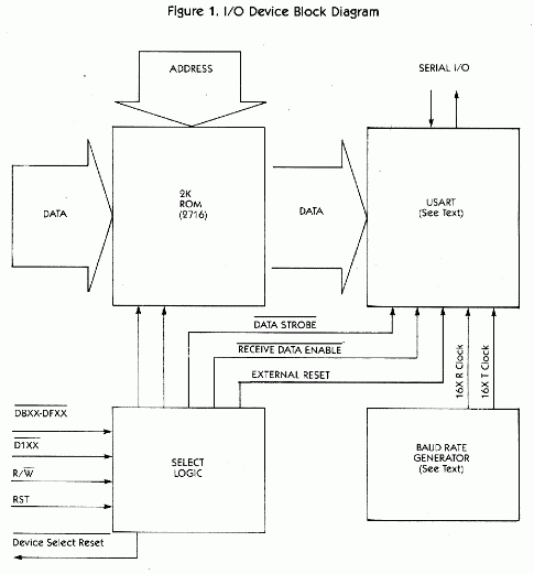
Figure 3. UART Pin Functions
| PIN | NAME (SYMBOL) | FUNCTION |
|
|
Power Supply (Vcc) | +5V Supply |
|
|
Not connected | |
|
|
Ground (VGI) | Ground |
|
|
Received Date Enable (RDE) | A logic "0" on the receiver enable line places the received onto the output lines |
|
|
Received Data Bits (RD8-RD1) | These are the 8 data output lines. Received characters are right justified: the LSB always appears on RD1. These lines have tristate outputs, i.e., they have the normal TTL output characteristics when RDE is "0" and a high impedance state when RDE is "1" Thus, the data output lines can be bus structure oriented. |
|
|
Parity Error (PE) | This line goes to a logic "1" if the received character parity does not agree with the selected parity. Tri-state. |
|
|
Framing Error (FE) | This line goes to a logic "1" if the received character has no valid stop bit. Tri-state. |
|
|
Over-Run (OR) | This lines goes to a logic "1" if the previously received character is not read (DAV line not reset) before the present character is transferred to the receiver holding register. Tri-state. |
|
|
Status Word Enable (SWE) | A logic "0" on this line places the status word bits (PE, FE, OR, DAV,TBMT) onto the output lines. Tri-state. |
|
|
Receiver Clock (RCP) | This line will contain a clock whose frequency is 16 times (16X) the desired receiver baud |
|
|
Reset Data Available (RDAV) | A logic "0" will reset the DAV line. The DAV F/F is only thing that is reset. |
|
|
Data Available (DAV) | This line goes to a logic "1" when an entire character has been received and transferred to the receiver holding register. Tristate-Fig. 16 |
|
|
Serial Input (SI) | This line accepts the serial bit input stream. A Marking (logic "1 ") to spacing (logic "0") transition is required for initiation of data reception. Fig. 15,16. |
|
|
External Reset (XR) | Resets all registers except the control bits register, Sets SO, EOC and TBMT to a logic "1". Resets DAV and error flags to "0". Clears input data buffer. Must be tied to logic "0" when not in use. |
|
|
Transmitter Buffer Empty (TBMT) | The transmitter buffer empty flag goes to a logic "1" when the data bits holding register may be loaded with another character. Tri-state. See Fig. 9, 11. |
|
|
Data Strobe (DS) | A strobe on this line will enter the data bits into the data bits holding register. Initial data transmission is initiated by the rising edge of DS. Data must be stable during entire strobe. |
|
|
End of Character (EOC) | This line goes to a logic "1" each time a full character is transmitted. It remains at this level until the start of transmission of the next character. See Fig. 8, 10. |
|
|
Serial Output (SO) | This line will serially, by bit, provide the entire transmitted character. It will remain at a logic "1" when no data is being transmitted. |
|
|
Data Bit Inputs (DB1-DB8) | There are up to 8 data bit input lines available. |
|
|
Control Strobe (CS) | A logic "1" on this lead will enter the control bits (EPS, NB1, NB2, TSB, NP) into the control bits holding register. This line can be strobed or hard wired to a logic "1" level. See Fig. 19. |
|
|
No Parity (NP) | A logic "1" on this lead will eliminate the parity bit from the transmitted and received character (no PE indication). The stop bit(s) will immediately follow the last data bit. If not used, this lead must be tied to a logic "0". |
|
|
Number of Stop Bits (TSB) | This lead will select the number of stop bits, 1 or 2, to be appended immediately after the parity bit. A logic "0" will insert 1 stop bit and a logic "1" will insert 2 stop bits. The combined selection of 2 stop bits and 5 bits/character will produce 1 1/2 stop bits |
|
|
Number of Bits/Character (NB2, NB1) | These two leads will be internally decoded to select either 5, 6, 7
or 8 data bits/character.
NB2 NB1 Bits/Character 0 0 5 0 1 6 1 0 7 1 1 8 |
|
|
Odd/Even Parity Select (EPS) | The logic level on this pin selects the type of parity which will be appended immediately after the data bits. It also determines the parity that will be checked by the receiver. A logic "0" will insert odd parity and a logic "1" will insert even parity. |
|
|
Transmitter Clock (TCP)
|
This line will contain a clock whose frequency is 16 times (16X) the desired transmitter baud. |
Figure 4. Baud Rate Generator
PIN FUNCTIONS
| PIN NO. | SIGNAL | DESCRIPTION |
|
|
XTAL/EXT1 | Input is either one pin of the crystal package or one polarity of the external input. |
|
|
Vcc | Positive power supply-normally +5V |
|
|
fR | This output runs at a frequency selected by the Receiver divisor select data bits. |
|
|
RA, RB, RC, RD | These inputs, as shown in Table 1, select the receiver output frequency, fR. |
|
|
STR | A high level input strobe loads the receiver data (RA, RB, RC, RD) into the receiver divisor select register. This input may be strobed or hard-wired to a high level. |
|
|
NC | |
|
|
NC | |
|
|
GND | Ground |
|
|
STT | A high level input strobe loads the transmitter data (TA, TB, TC, TD) into the transmitter divisor select register. This input may be strobed or hard-wired to a high level. |
|
|
TD, TC, TB, TA | These inputs, as shown in Table 1, select the transmitter output frequency ft |
|
|
ft | This output runs at a frequency selected by the Transmitter divisor select data bits. |
|
|
XTAL/EXT2 | This input is either the other pin of the crystal package or the other polarity of the external input. |
REFERENCE FREQUENCY 4.915200MHz
| Divisor
Select DCBA |
Desired
Baud Rate |
Clock
Factor |
Desired
Frequency (KHz) |
Divisor | Actual
Baud Rate |
Actual
Frequency (KHz) |
Deviation |
| 0000 | 50.00 | 16X | 0.80000 | 6144 | 50.00 | 0.800000 | 0.0000% |
| 0001 | 75.00 | 16X | 1.20000 | 4096 | 75.00 | 1.200000 | 0.0000% |
| 0010 | 110.00 | 16X | 1.76000 | 2793 | 109.93 | 1.758983 | 0.0100% |
| 0011 | 134.50 | 16X | 2.15200 | 2284 | 134.50 | 2.152000 | 0.0000% |
| 0100 | 150.00 | 16X | 2.40000 | 2048 | 150.00 | 2.400000 | 0.0000% |
| 0101 | 300.00 | 16X | 4.80000 | 1024 | 300.00 | 4.800000 | 0.0000% |
| 0110 | 600.00 | 16X | 9.60000 | 512 | 600.00 | 9.600000 | 0.0000% |
| 0111 | 1200.00 | 16X | 19.20000 | 256 | 1200.00 | 19.200000 | 0.0000% |
| 1000 | 1800.00 | 16X | 28.80000 | 171 | 1796.49 | 28.743859 | 0.1949% |
| 1001 | 2000.00 | 16X | 32.00000 | 154 | 1994.81 | 31.916883 | 0.2697% |
| 1010 | 2400.00 | 16X | 38.40000 | 128 | 2400.00 | 32.000000 | 0.0000% |
| 1011 | 3600.00 | 16X | 57.60000 | 85 | 3614.11 | 57.825882 | 0.3921% |
| 1100 | 4800.00 | 16X | 76.80000 | 64 | 4800.00 | 76.800000 | 0.0000% |
| 1101 | 7200.00 | 16X | 115.20000 | 43 | 7144.19 | 114.306976 | 0.7751% |
| 1110 | 9600.00 | 16X | 153.60000 | 32 | 9600.00 | 153.600000 | 0.0000% |
| 1111 | 19200.00 | 16X | 307.20000 | 16 | 19200.00 | 307,200000 | 0.0000% |
REFERENCE FREQUENCY=5.068800MHz
| Divisor
Select DCBA |
Desired
Baud Rate |
Clock
Factor |
Desired
Frequency (KHz) |
Divisor | Actual
Baud Rate |
Actual
Frequency (KHz) |
Deviation |
| 0000 | 50.00 | 16X | 0.80000 | 6336 | 50.00 | 0.800000 | 0.0000% |
| 0001 | 75.00 | 16X | 1.20000 | 4224 | 75.00 | 1.200000 | 0.0000% |
| 0010 | 110.00 | 16X | 1.76000 | 2880 | 110.00 | 1.760000 | 0.0000% |
| 0011 | 134.50 | 16X | 2.15200 | 2355 | 134.52 | 2.152357 | 0.0166% |
| 0100 | 150.00 | 16X | 2.40000 | 2112 | 150.00 | 2.400000 | 0.0000% |
| 0101 | 300.00 | 16X | 4.80000 | 1056 | 300.00 | 4.800000 | 0.0000% |
| 0110 | 600.00 | 16X | 9.60000 | 528 | 600.00 | 9.600000 | 0.0000% |
| 0111 | 1200.00 | 16X | 19.20000 | 264 | 1200.00 | 19.200000 | 0.0000% |
| 1000 | 1800.00 | 16X | 28.80000 | 176 | 1800.00 | 28.800000 | 0.0000% |
| 1001 | 2000.00 | 16X | 32.00000 | 158 | 2005.06 | 32.081013 | 0.2532% |
| 1010 | 2400.00 | 16X | 38.40000 | 132 | 2400.00 | 38.400000 | 0.0000% |
| 1011 | 3600.00 | 16X | 57.60000 | 88 | 3600.00 | 57.600000 | 0.0000% |
| 1100 | 4800.00 | 16X | 76.80000 | 66 | 4800.00 | 76.800000 | 0.0000% |
| 1101 | 7200.00 | 16X | 115.20000 | 44 | 7200.00 | 115.200000 | 0.0000% |
| 1110 | 9600.00 | 16X | 153.60000 | 33 | 9600.00 | 153.600000 | 0.0000% |
| 1111 | 19200.00 | 16X | 307.20000 | 16 | 19800.00 | 316.800000 | 3.1250% |