the toolbox
PARALLEL BUS REVEALED
100,000 bytes per secondPart II of a four part series
by EARL RICE
For the first time, advanced users of the Atari 800XL and 600XL. learn bow it's possible to connect peripherals to the fast, powerful Parallel Bus Interface. Part 2 of a 4-part series.
Last month we looked at the general operation of the Parallel Bus Interface
(PBI) emphasizing software concepts. This month, we'll look at the
hardware concepts involved in making an external device work via the parallel
bus.
Figure 1 shows the basic requirements for a simple serial
I/O function such as an RS-232 board. The serial I/O device can be
an integrated circuit that looks like a set of registers to the computer.
The decode logic selects the device when the assigned PBI addresses are
presented on the address bus.
Beyond that, the computer needs to be able to read and write
data to the device and respond to its requests for service. That's
what the Read/ Write and Interrupt Request lines are for.
When the computer wants to talk to a parallel bus peripheral,
it enables the decode logic with a signal called External Enable.
The decode logic decides whether the address on the bus is for the device
or for the 2K ROM.
If it's for the ROM, the decode logic returns a Math Pack Disable
signal to the computer so that internal ROM won't contend with the 2K ROM
for the data bus.
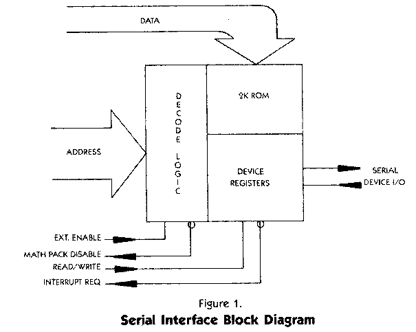
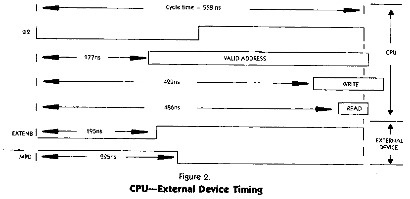
Figure 2 shows the approximate timing of the External
Enable (EXTENB) and Math Pack Disable (MPD) signals.
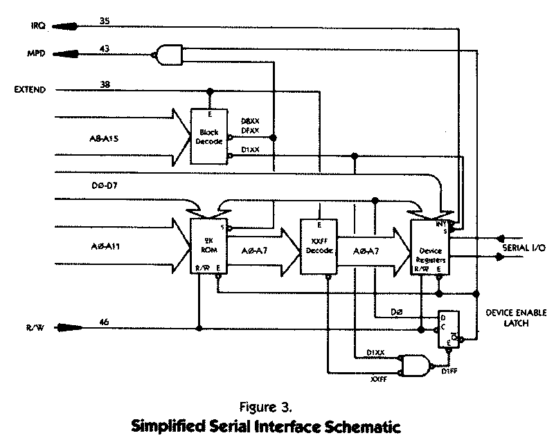
Figure 3 is a more detailed schematic of the hardware
example. This is still not the complete design, but it serves to
illustrate the concepts some more.
The decode logic does several things:
- Decodes the $D8XX-$DFXX block to enable the 2K ROM.
- Decodes the D1XX block for device registers.
- Decodes the address $XXFF so the computer can select the Device Enable latch at $D1FF. This latch represents the select bit in the Device Select register (DEVSEL).
The Device Enable latch must be set to allow the computer to address the 2K ROM or the device registers. Its output is also gated with the 2K ROM select line to send the MPD signal to the computer. The Device Enable latch is set by writing a I to $D1FF. It is reset by writing a 0 to $D1FF.
SUMMARY
The basic concept isn't hard. The external hardware is
enabled by EXTENB. It must decode the 2K ROM space, device registers,
and Device Select register. When the 2K ROM is selected, it must
return a Math Pack Disable signal to the computer. If the device
is interrupt driven, it must supply an interrupt Request(IRQ) to let the
computer know it. wants to be serviced. In that event it will also
need to supply an IRQ ID number to the computer.
Simple? Sure is ... At least at the conceptual level.
It gets a little more involved when we design the decoder and have to deal
with timing. We'll do that next month. In the meantime, here's
some additional information to help you understand the diagrams:
READING THE DIAGRAMS
Some of the signal names in Figure 3, have a bar over
them. That means the signal's active state is low (binary 0). The
little circles on the signal lines next to some of the symbols mean the
same thing. A dot at the intersection of two lines means they are
connected. If they cross without a dot, they aren't connected.
The wide arrows indicate multiple signal lines. The numbers inside
the arrows tell you which signals are involved. For example, the
arrow with A0-A11 means the address fines for address bit 0 through address
bit 11 all go to the 2K ROM. Only address bits A0-A7 go to the $XXFF
decoder and the device registers, however.
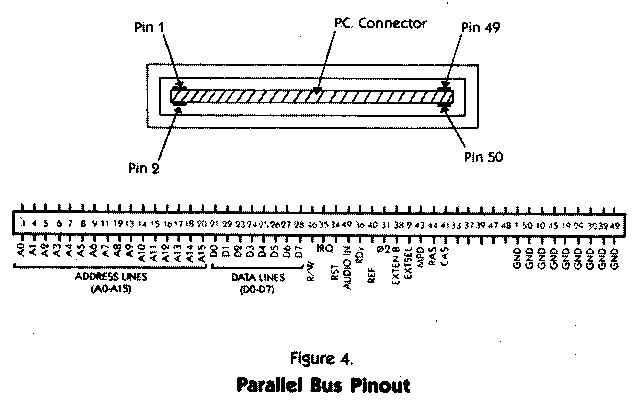
Figure 4 shows the pin numbers for the PBI signals.
It also shows how the pins are numbered on the printed circuit connector
at the back of your 800XL computer. Imagine you are looking into
the open connector slot.
CAUTION: Unplug your computer before removing the cover over
the slot. Be very careful not to short the connector pins.
Before touching a connector, be sure to discharge any static charge you
may have built up by touching a grounded conducting object (such as a cold
water pipe). STATIC CHARGES CAN DESTROY INTEGRATED CIRCUITS! BE CAREFUL!
Next month, we'll look at a serious design for a sort of baby
850 Interface-a serial I/O device useable for driving modems and such.
Earl Rice was head of users group support at Atari before moving on to be project leader of the now cancelled 1450XL computer