PRINTED CIRCUIT SCHEMATICS
Design PC Boards With DEGAS
BY THOMAS J. LYNCH, Ph.D
If you've ever spent time soldering or wire wrapping a one-of-a-kind circuit, you know the sinking feeling I get when someone asks, "How about building me one of those gadgets, too?" I recently built a device for an Army research institute. After months of wiring and troubleshooting, I swore that joining the circus and working without a net would he easier than building another one. Duplicates are sheer tedium, and with each one you run the risk of making wiring mistakes.
Take heart. Any high-rcz graphics program that can read and print the DEGAS-compatible .PI3 files on your START disk can make Printed-circuit (PC) design fun and eliminate the woes of duplication. (Follow the instructions in the READ_ME file on your START disk to un-ARC the picture files.) The ST does a fine job of drawing and printing a PC schematic, which is then used as the photo template for any of the commercial photographic-exposure methods of PC-board construction.
|
|
|
| Name:
Requirements: Arcfile: Files:
|
Printed Circuit Templates
512K, high rez, DEGAS SCHEMARC.PRG PCFORM1 P13 PCFORM2.P13 PCFORM3.P13 VCLAMP.P13 |
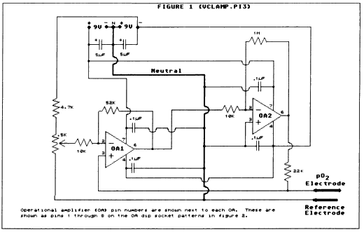
Figure 1: This
is an example of a symbolic circuit design which will be turned
into a printed circuit.
The symbols represent various electronic components
which will be soldered
onto the final product.
The Art Of Etching
Electronics magazines routinely dedicate a full page to one or more
PC schematics. If you want to make the schematic into a PC hoard, you would
do the following (this is a general description of the process, there are
variations). First, a picture is taken of the schematic to produce a positive
(the reverse of a traditional photographic negative) on a special film.
The film is then laid on top of a photosensitive, copper-plated PC hoard,
which is exposed to light for a precise period of time. Light which passes
through the transparent part of the film exposes the underlying copper,
while the copper under the dark image remains unexposed. When the entire
copper hoard is placed in etching solution (ferric chloride), all the light-exposed
copper is eaten away, leaving the unexposed copper creating the desired
circuit pattern. The advantage of this is that once you have a good PC
pattern, it's easy to build that circuit. All you do is photo-expose another
board, etch, plug in the components and solder. No wiring. No wiring mistakes.
With your ST, you can design and print as good a schematic as any done by the pros. PC kits containing the necessary materials for photo-exposing the hoard are available from vendors. (See sidebar.)
Board Design
Figure 1 is VCLAMP.P13 from the START disk. It shows a relatively
simple electrical schematic in symbolic form. Although this was drawn with
DEGAS, I find it easier and faster to do the symbolic schematics with a
pencil and paper. The PC schematic and final etched board must include
the battery power-supply lines leading to pins i and 7 of the operational
amplifiers, as well as the neutral return line (N), but it is convention
to leave these out of symbolic schematics. They are included in Figure
1 for the sake of clarity. An ON/OFF switch would also be needed in either
circuit but is not shown.
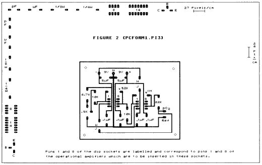
Figure 2: The
original symbolic circuit has been changed to this
printed circuit design.
The white areas represent where the copper
on the PC board will
be etched away.
Figure 2 is the PC version of Figure 1, and is called PCFORM1.P13. Figure 2 was done in about an hour by using DEGAS' copy function to move selected spacing patterns (for 1/8W resistor, F capacitor, etc.) from the margins to center screen. The line-draw functions in DEGAS let you make the connections to complete your PC schematic. If corrections in a PC schematic become necessary, the DEGAS picture file can be called up and altered much faster than a new version could he drawn by hand.
Compare Figures 1 and 2. In Figure 2, the symbols for resistors, capacitors and amplifiers are left out, but the spaces where they are to be soldered in place are labeled. Widened solder tabs are provided which, in the final etched board, are to he drilled so that the components can he plugged in and soldered. Load PCFORM1.P13 or PCFORM2.P13 and use a magnify mode (Fl key in DEGAS) to examine the pixel spacing in some of the PC patterns.
Figure 1 shows several semicircular crossings of one line over another. This is one convention for showing that the indicated conductors in the actual circuit are not to touch each other. In a PC schematic and the final etched PC hoard, there are three ways to keep conductors from touching each other when they must cross. The most sophisticated and difficult way is to etch both sides of a double-sided hoard, so that wherever there is an unavoidable crossing of conductors, solder connections through holes drilled in the hoard will effect the crossover. This method is not dealt with here. The second way is to use a resistor or capacitor to cross over the conductor: see the 52K and 1M feedback resistors of Figure 1 and notice that they jump the neutral and supply lines in Figure 2. Where there is no resistor or capacitor to take advantage of, you can use a simple wire jump (WJ). Figure 2 includes two wire jumps. In the final etched board, each WJ becomes a small piece of bent wire, such as part of a resistor lead. Each is plugged in and soldered to span the gap.
Drawing a PC schematic is similar to working a two-dimensional puzzle in which you try not to get boxed into a wire jump. Can you find a way I might have rerouted conductors to avoid the two wire jumps in Figure 2? As you gain experience with the technique, you will notice that the simplicity of a wire jump may be preferable to the complexity of a route which avoids it.
Practice Makes Perfect
Printed-circuit design is not a difficult process. If you can draw
an electrical schematic, analog or digital, you can design a PC schematic.
Even if you don't have the background to draw the initial symbolic schematic,
you can take an existing one and translate it into the PC format. However,
if you have never done this before, start with a schematic containing no
more than one or two integrated circuits.
Before tackling your own project, practice. Use DEGAS Elite or a compatible graphics program to load PCFORM3.PI3 from the START disk and start translating the symbolic schematic in VCLAMP.P13 into PC format. After a few hours practice, you will find it easier to handle your own circuits.
PCFORM3.P13 is a blank picture, with PC pictures for resistors, capacitors and dip sockets lining the margin. Move them into the center of the screen, erase their labels and connect the solder tabs to each other with the line-drawing function. You can compare your version with mine in Figure 2, or just try to copy it for practice. If yours looks different, that's fine, as long as all components are accounted for. There is no single solution to the puzzle. After doing several PC schematics of increasing complexity, you should find some amusement in examining PCs designed by professionals. Notice that they too get stuck and sneak in an occasional wire jump.
|
|
| If you have never etched a PC board, please
read the kit instructions thoroughly, and follow them exactly. Better yet,
find someone experienced in PC-board making and have them help you. Using
acids and other toxic chemicals is dangerous. Finally, send for catalogs
and do some comparison shopping before ordering. A typical kit costs about
$40.
Bishop Graphics, 5388 Sterling Center Drive, Westlake Village, CA 91359 The DATAK Corporation, 3117 Paterson Plank Road, North Bergen, NJ 07047 Kepro Circuit Systems, 630 Axminster Drive, Fenton, MO 63026-2992 Vector Electronic Co., 12460 Gladstone Ave., P0 Box 4336, Sylmar, CA 91342-0336 |
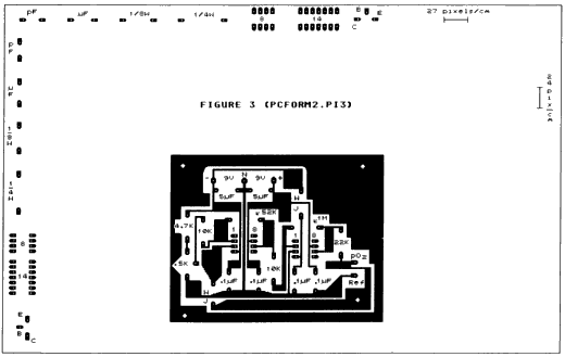
Figure 3: This
circuit is the same as Figure 2 except that selected areas have
been filled in so that
less copper will be etched from the board, making the
process faster and less
wasteful.
When the schematic is printed on paper (using 8.5- by 11-inch standard printer drivers), you should find that the pattern elements are spaced properly for the wire leads of standard-sized resistors, capacitors and dip sockets, and should therefore serve as a good photo template. Since DEGAS has additional text capability, it's easy to annotate the PC schematic so that the solder tabs on the final etched board will be labelled with the respective component. Such labeling makes the solder/assembly process easier and adds a professional touch to the final board.
Making Adjustments
In Figure 2 and the corresponding disk file, notice that the margins
contain both horizontally- and vertically-oriented PC spacing patterns
for the same electrical components. These are for the two ways that components
are generally soldered into a PC hoard. For any particular PC pattern,
the pixel spacing for the horizontal and vertical versions is slightly
different. This is because the same number of pixels printed horizontally
takes up less paper space than when printed vertically.
In addition to resistor and capacitor spacing patterns, the margins of the disk files contain patterns for 8-and 14-pin dip sockets, and for a standard-size transistor (labelled E, B, C for emitter, base and collector). There are also millimeter rulers for horizontal and vertical measurement. These can be used to make your own patterns for other electrical components of different sizes. To do this, for example. for a large capacitor, measure the distance between the leads with a real millimeter ruler, and add tip the total number of pixels this equals on the bottom (horizontal) or left (vertical) side of the appropriate screen ruler. When you have the total for the desired orientation, magnify a blank part of the PCFORM3.P13 screen. Now use the mouse to draw an assembly of pixels forming one solder tab, then draw a straight line away from this tab, counting the pixels as you go. When you reach the required distance, draw the second solder point. Print the screen and hold the capacitor up to your new pattern. If the spacing is correct, go hack to your screen and erase the counting pixels from between the solder tabs, then copy the new pattern to the margin. The particular pattern spacings shown here are customized for a Panasonic 109 ii printer. If you have a different printer, you may have to adjust the pixel spacing.
For Best Results.
In printing a PC schematic for photo-exposing a copper board, the schematic
ink should he as dark as possible. Use a new ribbon. A worn out ribbon
whose print is too light may result in gray areas on the film and partial
exposure of parts of the hoard intended to he conductors. Since the exposure
time of photosensitive boards is critical to within three seconds, it's
wise to dedicate a ribbon to PC schematics.
Also, when you print, examine the printed figure for white lines in areas that are supposed to he black. Sometimes the printer will roll the paper a little bit too far, leaving a thin white streak. Fill in any such area by hand with black pen ink.
Figure 3 (PCFORM2.P13) is the same PC schematic as Figure 2 but with many of the separate conductors widened. This is optional, but it results in less of the copper board being exposed, and therefore less copper being etched away when you put the hoard into the ferric chloride solution. Why should you be concerned with this? If you minimize the copper etched per board, you will be able to etch more hoards per solution. Many commercial, digital boards arc not filled in like Figure 3 because they are just too complicated.
To widen the conductors as in Figure 3, use DEGAS' line-drawing function to enclose an area, choose a solid black fill pattern, then fill the selected area. Be careful that widening the conductors does not create an electrical short between any conductors which must be isolated from each other. Also, remember that if you try to fill an area that is not completely pixel enclosed, it will leak out and fill much of the screen. If this happens. hit the UNDO key in DEGAS and your mistake will he undone.
Thomas Lynch holds a doctorate in neurophysiology and is a professor at Temple University in Philadelphia.