Building SAMPSYN
A Hardware How-To
| GETTING STARTED | |
|
| SAMPSYN PARTS | ||||||||||||
|
||||||||||||
|
||||||||||||
 START VOL. 4 NO. 12 / JULY 1990
Building SAMPSYNA Hardware How-To
|
|||||||||||||||||||
Sampsyn is not a beginner's project. If you're not experienced with electronics, you'll need the help of someone who is.
The Sampsyn prototype was constructed on a large 2-bus circuit board using point-to-point wiring. The interface was built on a separate cartridge plugboard, and the two boards were connected with a 16-conductor DIP jumper cable.
Since both digital and analog circuitry are combined on the board, they each need separate ground returns. Otherwise, digital switching noise can bleed into audio output. The schematic denotes the digital ground with the conventional three-line symbol, and the analog ground with the letter A enclosed in a triangle. The only point at which the two grounds meet is the power supply junction on the board.
The analog circuitry requires an external power supply which can range from +9 to +15 VDC. An inexpensive DC wall-outlet adapter is sufficient. Sampsyn obtains its +5V power supply from the computer.
While you're assembling Sampsyn, keep the component leads and wire jumpers as short and direct as possible. Don't bundle the wires or else you'll get crosstalk. Use sockets for all ICs and shielded cable for connecting audio input and output jacks to the circuit board--connect only one end of the shield to ground. Check for solder bridges and cold joints; observe proper polarity of diodes and electrolytic caps, and don't use too much heat on semiconductors. Before inserting the ICs, check your connections with an ohmmeter.
Housing the circuit in an aluminum chassis box keeps it safe, and shields the audio circuitry from external noise.
The first part of this tutorial refers to the the first schematic (Figure 1).
First of all, before digitizing the audio input with the analog-to-digital converter IC3, you can boost it at J1 with a pre-amplifier IC1A and condition it with a compressor IC2A.
The AD7575JN is a successive approximation converter. It converts in six microseconds with a 3.579 MHz clock input (provided by the oscillator built around NOR-gate stages IC4A, B and C, and crystal XTAL 1).
To initiate data conversion, use your computer to lower the pulse of pins 1 and 2 of IC3. Twenty clock cycles later, the chip's internal register stores an 8-bit binary representation of the analog input. Your computer reads the data by strobing pins 1 and 2 low again, enabling the register's tri-state output buffer and restarting data conversion.
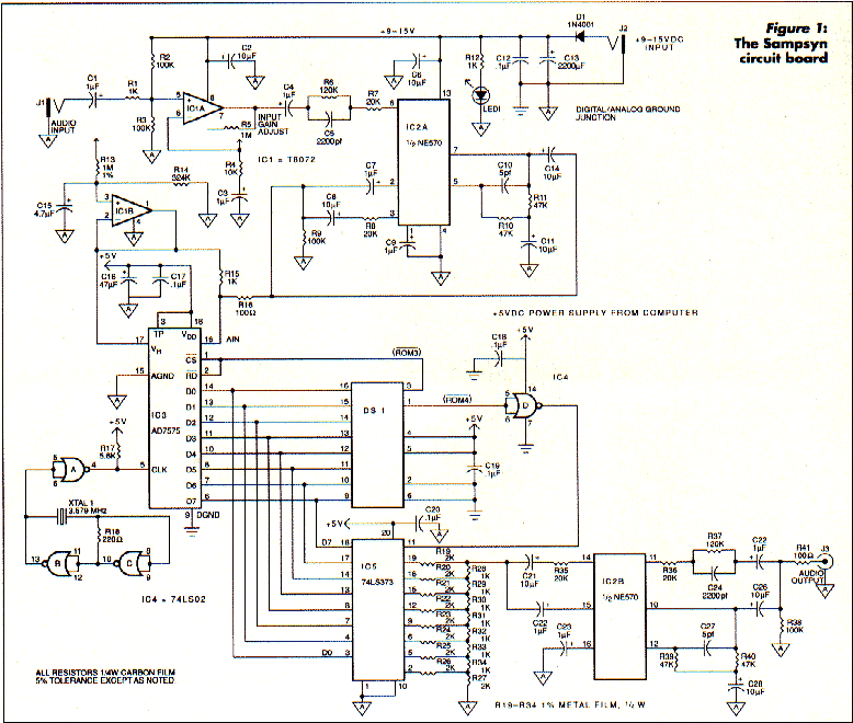 |
To construct the digital-to-analog circuit, use an 8-bit data latch (IC5) and an "R-2R" resistive ladder (R19-R34). Strobe data from the computer into the latch by pulsing enable pin 11 on IC5 high. The resistor network divides logic-level signals when latch outputs to binary-weighted currents; the result of this division appears at the junction of R19 and R28. You can suppress quantization noise with the IC2b expander and IC2a.
The second schematic refers to the cartridge port interface (Figure 2). A pinout of the ST's cartridge port (Figure 3) will help orient you. The view is external, as if you were looking straight at it.
The cartridge port is memory-mapped from addresses $FA0000 to $FBFFFF. This lowers the pulse of the port's ROM3 pin during any read operation (i.e. a PEEK in BASIC) from $FA0000 to $FAFFFF, and the pulse of the ROM4 pin from addreses $FB0000 to FBFFFF.
ROM3 is connected directly to both the CS and RD pins of the analog-to-digital converter. Reading address $FA0000 is really reading the contents of the converter's output register, which restarts the conversion for the next read operation.
Connecting the digital-to-analog converter to the ST presents a special problem, since the cartridge port was designed solely as a read-only interface. Any attempt to write to (i.e. POKE) the cartridge address range causes a bus error and, ultimately, a crash. So how do you pass data to the D/A converter?
Paradoxically, place the data on the lower address lines during a read cycle (rather than the data bus during a write), and invert ROM4 to strobe the data into the D/A latch from the address bus. Since any address from $FB0000 to $FBFFFF pulses ROM4, you can place data that you want to send to the DAC onto address lines A1-A8 and read from address $FB0000+[data*2]. For example, the BASIC statement:
X=PEEK(&hFB0002)
sends a value of one to the D/A converter. Before it's placed on the address bus, the data byte is multiplied by two (shifted left one bit). Since reading from an odd address is illegal to the 68000, this ensures that the address is an even number.
Use octal buffers IC6 and 7 to combine input and output lines from the cartridge port into a single 8-bit bus. This is not a requirement, since data lines D0-D7 can go directly to the AD7575 and A1-A8 can go directly to the 74LS373. But it is necessary if you want a circuit with a general-purpose interface for bus-oriented peripherals. You can omit ICs 6 and 7, but you'll need a cable with at least 20 conductors to carry the eight data lines, eight address lines, ROM3, ROM4, five volts, and ground from the interface card to Sampsyn.
To play with Sampsyn, connect the interface card to Sampsyn with a 16-pin DIP jumper cable. With your computer off, plug the interface card into the ST cartridge slot and the external power supply into Sampsyn's power supply input jack (J2). The power-on indicator LED1 should light up. Now turn the computer on. Plug a microphone or line-level output into the audio input jack (J1). Set input gain pot R5 all the way up for a microphone, and all the way down for line input. You should be ready to go.
|
|||
|