SOPHISTICATED HARDWARE TECHNIQUES FOR THE EXPERT
by G. Stewart Beal
Your cartridge port isn't just for cartridges anymore. ST developer G. Stewart Beal shares a hardware technique-complete with pictures, timing diagram, and schematic-to turn your cartridge port into a high-speed I/O port. So read on and leave the domain of "Read Only."
A crash of static punctuates the warbling tones emanating from the speaker of your amateur radio transceiver and an unsightly streak appears on the otherwise perfect color image received from a fellow Ham 10,000 miles away. The signal fades, and you are left staring at the marred record of an exciting contact you had waited months for, using amateur Slowscan Television. But your disappointment fades as you realize the image can be fixed. You move the mouse and click on the image-processing function button. You apply a median filter to the affected region then click the painter button and pull up fat-bits. You quickly color the bad pixels with 'transparent" paint, add several inferior low-resolution images received earlier, averaging their good parts over the blemish and-viola! -an almost perfect image to save to disk as a memento of the contact.
You can do this now. Input an image with over 250,000 colors from a TV camera, VCR, or directly off the air; use sophisticated mathematical functions to enhance the subject; title the picture from some 160 fonts; then send the image anywhere by phone, radio or satellite link. It's all done with a small, image-display box called a Scan Converter to which your personal computer talks through a parallel port. Together, they make up an exciting tool for communicating ideas.
Bill Montgomery (VE3EC) and I developed the software for this low-cost image-processing system using an IBM PC clone and a Robot Research 1200C color scan converter (R1200C). The scan converter is a 256 pixel by 240 line image-display system with 18 bits per pixel and some local intelligence. The software for the PC (called GEST: a Graphics Environment for Slowscan Television) permits loading and saving images and fragments, has a painter module with vector and bit-mapped fonts, and permits numerous image-processing operations for filtering, classifying, and feature extraction. When the Atari ST first came out, we immediately realized its price/performance ratio was much more attractive than the PC's. A tempting environment to convert our system to. So, why not try it?
The R1200C needs two unidirectional, eight-bit I/O ports and some additional control and status lines. Ultimately, the approach I took for the ST version was to build something which plugged into the then unused cartridge port, offering ready access to the high-speed transfers required.
SEARCHING FOR A PORT
Writing the GEST package for the IBM PC consumed a lot of time but the effort provided us with several new image-communication tools. The additional horsepower of the ST's 68000 processor would increase the speed of many of the image-processing operations, such as a low-pass filtering which requires approximately 1.8 million multiplications and divisions. Our main problem with transferring the system from the PC to the ST was the interface. On the PC, we had used straightforward interface cards since the bus is available through plug-in slots on the motherboard. But there are no such general-purpose connections on the ST, so I began investigating its higher speed access points: DMA, parallel printer port, and cartridge slot.
Initially, the printer port seemed attractive. I could build a device which would generate two unidirectional eight-bit ports from the bidirectional one available, but it would require an additional signal to inform the device of the port's current data direction. A user-accessible bit (called GPO, for General Purpose Output) was available on the monitor socket. It could be taken from there or wired across to an unused pin on the DP-25 printer connector inside the ST. But this approach would require either a special cable for the monitor connector or a modification of the ST hardware, both of which might lead to future incompatibilities. Thus, the printer port was rejected as an access point.
The DMA port offered the tempting advantage of simultaneous data transfer and processing. But it looked too scary to tackle since there was little information on the protocol used, and it would require an intelligent device to supervise the transfers to and from the R1200C.
The cartridge port remained to be examined. It looked good. No modification of the machine was needed (the device could be completely removed), and no other cartridges were available at the time, so the socket was free. One major problem with the cartridge interface was the lack of any signal to convey the data direction (read or write). The slot is designed to accomodate "read only" memory devices; the only operation permitted is input. In fact the ST's Memory Management Unit (MMU) generates system exceptions when programs attempt to write to the region of memory occupied by the cartridge.
There seemed to be no simple way to interface an Atari ST. Then I noticed the large number of connections at the cartridge slot: 16 data-bus lines, 15 address lines, 2 data strobes, and 2 ROM-select lines. Nor only were there many signal lines, there were both inputs (the data bus) and outputs (address lines, strobes and selects). The means of conveying the information to the interface along the address lines was the only thing holding me back.
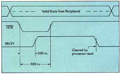
FIGURE 1: typical 8255 Input Handshake Timing.
CARTRIDGE THEORY
Consider the way the ST cartridge is meant to operate. The ROMs used in most cartridges store bytes of information organized in a byte wide fashion. That is, each access to the ROM returns a full eight bits of information in parallel. Since the Atari ST systems are word oriented (they can transfer 16 bits of information in or out at a time) the simplest means of building cartridges is to use pairs of ROMs-one providing the low-order, eight-bit byte, and the other the high-order byte. The 68000 processor, however also permits access to single bytes of the memory and provides data strobe signals to indicate the particular byte desired: the Upper Data Strobe (UDS) and the Lower Data Strobe (LDS). When the processor wants a full 16-bit word, it asserts both signals simultaneously, activating both ROMs of the pair which then present their output data.
To distinguish among the many bytes of data contained in the ROMs, we rely upon each byte's address. Each ROM has several pins called address lines and when these lines are set up with various combinations of high and low voltages, specific locations are accessed for their bytes. The highs and lows correspond directly to the ones and zeros in the binary representation of the address number.
The address space of the cartridge ROMs is located in ST memory from $FA0000 thru $FBFFFF (128K bytes decimal). Since the largest commonly available ROMs contain 32K bytes, four are needed to completely fill this space. Since only 15 address lines are passed to the cartridge, we still need some way to access the full 128K. The cartridge, therefore, is provided with ROM-select signals which determine which pair to access. ROM4 is asserted if the desired address falls between $FA0000 and $FAFFFF, while addresses $FB0000 thru $FBFFFF cause ROM3 to be asserted. These ROM select lines, decoded and provided by the MMU, eliminate the requirement for passing the full 23 address lines to the port and the corresponding logic on the cartridge to interpret them.
So what do we have to work with? There are 16 lines to transfer input to the computer (data bus) and 15 lines on which information might be moved to the interface for output (address bus). If we make use of the ROM-select lines to tell us when to activate the interface, all the address lines can be used to transfer information. Normally, one doesn't think of a program having control over the address bus since the processor is driving it to fetch the instructions and data. But consider what happens if a request for a specific byte from one of the ROMs in a cartridge is made (the byte at $FB01FE for example). The CPU asserts the address lines to generate $FB01FE, and assert UDS to indicate that a byte from the even ROM is desired. The top eight address lines (which convey the bank information, $FB) connect to the MMU where it is determined that ROMselect line 3 needs to be asserted. The remaining address lines convey the value $01FE to the cartridge. If we consider these address lines as an outbound data bus, it is apparent that we can write the data value $01FE by reading from address $01FE.
Once I had determined how talk to the scan converter, all that remained
was to design and build the interface. I found the design to be simple,
but the construction posed a problem because the cartridge connector chosen
by Atari had unusual pin spacings: two millimeters, center to center None
of the many catalogs I consulted listed any prototype cards with pre-etched
fingers of these dimensions. The solution was to make my own adapter. (A
custom connector is no longer needed since prototype cards are now available.
See Reference.) The details of how I built the connector are presented
later in the article for reference. The technique is simple and doesn't
require any artwork for the printed circuit connector.
| Pin |
|
Direction | Pin |
|
Direction |
| 1 | Power +5VDC | to cartridge | 22 | Address 14 | to cartridge |
| 2 | Power + 5 VDC | to cartridge | 23 | Address 7 | to cartridge |
| 3 | Data 14 | from cartridge | 24 | Address 9 | to cartridge |
| 4 | Data 15 | from cartridge | 25 | Address 6 | to cartridge |
| 5 | Data 12 | from cartridge | 26 | Address 10 | to cartridge |
| 6 | Data 13 | from cartridge | 27 | Address 5 | to cartridge |
| 7 | Data 10 | from cartridge | 28 | Address 12 | to cartridge |
| 8 | Data 11 | from cartridge | 29 | Address 11 | to cartridge |
| 9 | Data 8 | from cartridge | 30 | Address 4 | to cartridge |
| 10 | Data 9 | from cartridge | 31 | _ROM3 Select | to cartridge |
| 11 | Data 6 | from cartridge | 32 | Address 3 | to cartridge |
| 12 | Data 7 | from cartridge | 33 | _ROM4 Select | to cartridge |
| 13 | Data 4 | from cartridge | 34 | Address 2 | to cartridge |
| 14 | Data 5 | from cartridge | 35 | _Upper Data Strobe | to cartridge |
| 15 | Data 2 | from cartridge | 36 | Address 1 | to cartridge |
| 16 | Data 3 | from cartridge | 37 | _Lower Data Strobe | to cartridge |
| 17 | Data 0 | from cartridge | 38 | Ground | to cartridge |
| 18 | Data 1 | from cartridge | 39 | Ground | to cartridge |
| 19 | Address 13 | to cartridge | 40 | Ground | to cartridge |
| 20 | Address 15 | to cartridge | |||
| 21 | Address 8 | to cartridge |
THE INTERFACE
The unit I designed provides the necessary logic to interact with the signals present on the cartridge port. It also handles data and control to and from the scan converter. There are two eight-bit data pathways, one each for input and output, so the unit is capable of operating in full duplex (sending and receiving simultaneously). Synchronizing information for each path is provided by a control line called a strobe and a status line called a busy. The data sender uses the strobe line to show valid data is being transferred, while the receiver uses the busy line to indicate readiness to accept the data from the sender. Because the strobe signals are often short pulses, the input path is provided with a holding latch which sustains the signal until it can be detected. Additionally, a status register, readable by the ST, is provided to store information about the strobe and busy lines for each path.
The interface was designed to simulate an 8255-type Programmable Peripheral Interface (PPI) chip operating in strobed input mode (see Figure 1 ). Data for input to the device is presented on the input lines, then the input strobe line (-ISTB, a low-true signal) is asserted. The PPI then asserts the busy line (IBUSY, high-true), indicating the data has been captured, and clears it when the input register is read by the processor. The complementary output operation must generate the output strobe (-OSTB, low-true) and use the busy line, now called acknowledge (OACK, high-true), to sense readiness in the external hardware.
The design of the scan converter permits only a single pixel (picture element) to be written to the screen each time a horizontal line is scanned. This theoretically permits nearly 50,000 bytes of data to be moved each second (one byte each for red, green and blue times 15,750 scan lines per second), but in practice, only about 20,000 bytes per second are sent or received. This is because a processor in the scan converter is watching the status lines in much the same way as the ST computer is: the latent time between the strobe being set and the processor retrieving the data is totally lost. This consideration should enter into data rate calculations before deciding to use this interface for high speed communication.
TALKING TO THE OUTSIDE WORLD
There are several operations to be considered in programming the interface to talk to the external hardware. It is always necessary to ensure the readiness of the device to accept input or provide output. The status register fulfills this synchronization requirement. When the scan converter wishes to send the interface a byte of data, it first looks at the busy line to see if the computer can accept the byte. If so, it places the data on its outbound data port and asserts the strobe line. This causes the interface to capture the byte and to set a bit in its status register. The computer periodically polls the status register by reading a location in the cartridge address space. If there is a byte available, it can fetch it from another location. The data input operation, in turn, clears the busy line to the scan converter, indicating the interface can accept another byte.
Output to the interface is slightly more complicated but also relies on a busy line, this time from the scan converter When the program wants to send a byte, it reads the same status register but examines a different bit to determine the readiness of the scan converter. When it knows that the unit will accept the byte, it prepares to write it to the interface. The byte to be written must be shifted left one bit (since the least significant bit of the address is not provided to or used by the cartridge), yielding an offset value. This value is added to the base address of the interface output port, forming a new address which is also in the cartridge address space. A read is then performed on this address and, magically, the data byte appears on the output and the strobe line is asserted.
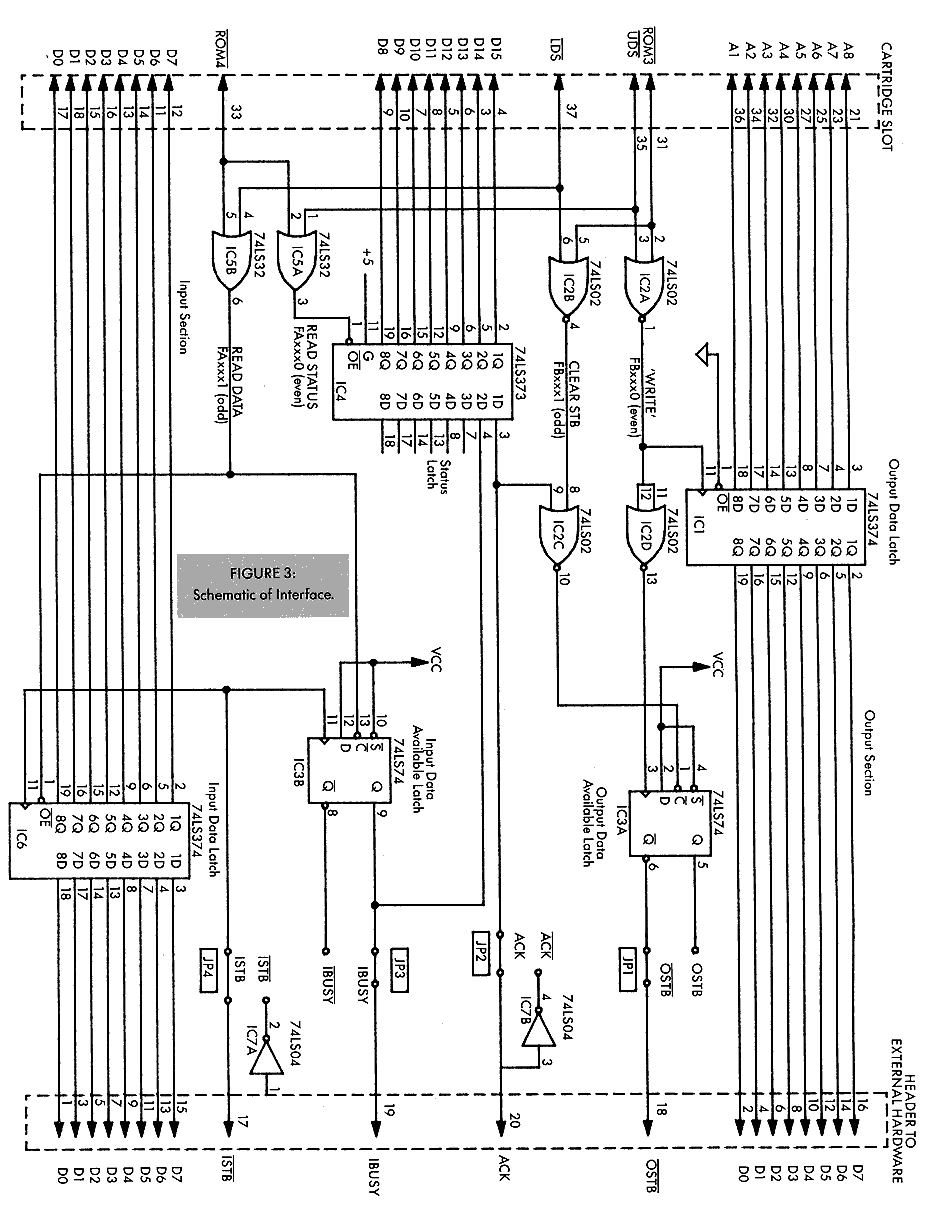
THE HARDWARE
Since the interface plugs into the cartridge port and there is no other use for the memory space occupied, no minor address decoding is performed.
The interface requires only four control signals: read status, read data, write data and clear -OSTB. The signals for input operations (read status and read data) are derived from the -ROM4 line together with -UDS and -LDS at IC5A and IC5B. These signals correspond to reads at byte address $FA0000 (or any even address in the $FAxxxx bank) for status and $FA0001 (or any similar odd address) for data. Analogously, signals for output (write data and clear -OSTB) come from -ROM3, -UDS and -LDS at IC2A and IC2B. Reads at even addresses in the $FBxxxx bank perform the write operations, while a read at any odd address will clear -OSTB.
$FAxxxx was chosen as the address block for the input section because the ST operating system attempts to read a magic number from the first four bytes of the cartridge ($FA0000 - $FA0003) early in the boot procedure. This is done to detect and transfer control to an executable program resident in the cartridge. If the output section was assigned there, spurious data would be written to the external hardware. The added benefit of having the input section at $FAxxxx is that two reads ($FA0001 and $FA0003) will be generated by the boot process which will clear the input data status latch in case turn-on transients in the external hardware caused an apparent data transfer into the input latch.
There is one fly in the ointment, however: The least significant bit (LSB) of the address is not available directly on the bus (see Figure 2 ). Fortunately, since we only need eight bits, and the cartridge is 16-bit word oriented, the LSB is not required. The interface could have used the UDS and LDS signals to form the least significant bit, but due to other considerations, address bits A8 through Al were used instead. This requires a one-bit left shift of the data to be written before the address calculation.
The remaining signals can be separated into two groups: D15 through D8, and D7 through D0. These lines make up the data bus, and I split them to emphasize the byte-oriented nature of the interface. The low-order eight bits provide the input data while the high-order bits provide the status of the latches to the computer (Internally, the 68000 moves data from D15 through D8 to the low end of a register when a byte access to the high byte is requested, so it was unnecessary to multiplex the status and input data latches to the low data bus.)
The -ISTB/IBUSY and -OSTB/OACK signals are handled by d-type latches in the interface (see Figure 3 ). In the case of the input section, the leading edge of the strobe causes the data on the input lines to be captured and the input data available latch (IC3B) to be set. The state of this latch is passed back to the external hardware as IBUSY and to the status port (1C4) for reading by the processor.
In the output section, the data to be written (present on A8-A1) is captured in the output latch (IC1) on the leading edge of the processor WRITE signal. The trailing edge of this signal (generated by inversion in IC2C) is used to clock the output data available latch (IC3A) to provide -OSTB to the external hardware. The separation in time of these two edges permits the write data to propagate through the output data latch and to become stable before -OSTB is generated.
For the input section, the external hardware should sense IBUSY to ensure
the latch is free to accept data. This line is cleared as the ST processor
retrieves the input data from the data latch (IC6). The output section
functions similarly, except the leading edge transition of OACK (in fact
the external hardware's IBUSY) is passed through IC2D and causes -OSTB
to be reset. OACK is routed to the status port and its trailing edge signifies
the external device is ready to accept more data.
/*
        this routine dumps the R1200C image memory to the screen
        buffer array 'src_buf', switches bank in the R1200C, then
        reloads the image back.
*/
#include "stdio.h"
/*
        define R1200C commands
*/
#define DUMP_RAW 0xBD
#define BANK_INC 0x03
#define LOAD_RAW 0xFD

usigned char scr_buf[200000];  /* the screen buffer */
main()
{
unsigned char red, green, blue, get1200();
register unsigned char *bp;
register long 1;

        flush1200()    /* clear the interface */
        printf("\nany key to dump screen to buffer");
        bp = scr_buf;
        getchar();     /* wait for the user's signal */
        printf("\ndumping");
        put1200(DUMP_RAW);     /* ask R120C for the current image in R,G,G */

        for (i=01; i<101; i++ <    /* show the first 10 pixels */
                *bp++ = (red = get1200());    /* red */
                *bp++ = (green = get1200());  /* green */
                *bp++ = (blue = get1200());   /* blue */
                printf("\nr = %d, g = $d, b = %d", red, green, blue);
        }

        for (i=101; i<614401; i++) <
                *bp++ = get1200();        / red */
                *bp++ = get1200();        / green */
                *bp++ = get1200();        / blue */
        }

        put1200(BLANK_INC);     /* go to the next bank in the R1200 */

        printf("\nany key to re-load screen");
        bp = scr_buf;
        getchar();             /* wait til user is ready to watch */
        printf("\nloading");

        put1200(LOAD_RAW);     /* ask R1200C to receive the R,G,B image */
        for (i=01; i<614401; i++) {
                put1200(*bp++); /* red */
                put1200(*bp++); /* green */
                put1200(*bp++); /* blue */
        }
        printF("\ndone");
}

/*
        define addresses of the ports on the interface
*/
static unsigned char *r1200in = 0xFA0001; /* input data read from here */
static unsigned char *r1200st = 0xFA0000; /* I/O status read from here */
static unsigned char *r1200ou = 0xFB0000; /* data xx written when read from
                                             (here + (xx<2)) */
static unsigned char *r1200ou = 0xFB0001; /* output strobe cleared if read */
/*
        define the status bits on the interface
*/
undefine INREADY 0x40
undefine OUTREADY 0x80

flush1200()     /* routine to clear the interface */
{
register unsigned char c;
        c = *r1200in:   /* clear the input register and status */
        c = *r1200oc;   /* clear the output strobe */
        return;
}

put1200(c)       /* routine to send data to the output port */
char c;
}
register unsigned char *cp, cc;
register int 1i;

        ii = c * 2;                     /* product bigger than byte */
        (p = r1200ou + (ii & 0x1FE);    /* calculate address */
        while (*r1200st & OUTREADY);    /* wait til ready */
        cc = *cp;                       /* write the byte */
        return;
}

unsigned char get1200() /* routine to receive data from the input port */
{
        while (!(*r1200st & INREADY));  /* wait for data available */
        return *r1200in;                /* get the byte and return it */
}
|
PROGRAMMING
The simplest way to demonstrate the operation of the hardware is to use BASIC in immediate mode. Some form of an indicator is required to show the operation of the card. A scope is ideal but a logic probe, even without a pulse detector, may be used. The first section to debug is the status circuitry at 1C4. The computer may read this at location $FA0000 by issuing the following commands:
DEF SEG = &HFA0000
I = PEEK(0)
The first command tells BASIC the base address of memory operations (and sets up to do byte-sized rather than word-sized accesses). The second command actually reads the status port (offset zero from the base). Printing I will show the state of the input bits on 1C4. The number printed will have a bit set for each of the bits in the input port which are high. The number printed will be at least 63 because the low six bits on the port are un-terminated and will assume a high state due to internal biasing on the chip. These lines could be tied low to generate zeros, but I simply ignore them. If, for example, the value of I were 255, it would indicate all inputs were high including those from the OACK line and the IBUSY line. This can be verified using the indicator.
The next thing to verify is that the status port indicates the true states of the lines. OACK can be clamped high or low to demonstrate its operation but the IBUSY line may only be set with an appropriate transition on the ISTB line. Assuming the current DEF SEG is &HFA0000, IBUSY is cleared by reading the data input port as follows:
I = PEEK(1)
To verify the correct operation of the input, various input lines may be tied high and low in known patterns (alternates, pairs, top four, etc.) then the ISTB line can be pulsed. The status port should indicate the data is now available using a PEEK(0) and the data may be read with a PEEK(1). Following the data read, the IBUSY line should return to its inactive state.
Output operations are slightly more complicated. The base address for operations is set to $FB0000 with the command:
DEF SEG = &HFB0000
To write a data value of X, issue the command:
I = PEEK(2*X)
The value returned to I is meaningless. Verify that I = PEEK(0) clears all bits in the output port while I =PEEK(510) sets them all (510 = 2 * 255). Similar experiments should validate that all bits function individually.
The operation of the output data-available latch and OSTB can be verified by observing that IC3A pin 5 goes high when the PEEK from any even offset is issued and that it goes low again if either the OACK line is toggled or a PEEK from an odd offset is issued.
Once these operations have been demonstrated, the interface may be configured and connected to the external hardware for use.
The commented listing in Figure 4 illustrates use of the device from the C language and should require no further explanation.
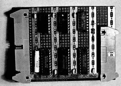
FIGURE 5: Photograph of Component Side of Interface.
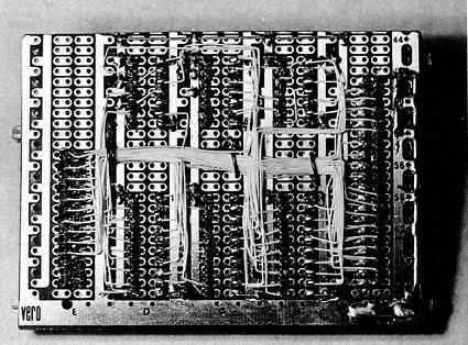
FIGURE 6: Photograph of Wiring Side of Interface.
|
|
Vcc | GND | |
| IC1,6 | 74LS374 | 20 | 10 |
| IC2 | 74LS02 | 14 | 7 |
| IC3 | 74LS74 | 14 | 7 |
| IC4 | 74LS373 | 20 | 10 |
| IC5 | 74LS32 | 14 | 7 |
| IC7 | 74LS04 | 14 | 7 |
ASSEMBLY AND TROUBLESHOOTING
The first interface was built on a small piece of Vero-perforared prototype card using point to point soldered wiring with 28-gauge wire-wrap wire. Figure 5 and Figure 6 show the front and back of the card. The external hardware is connected to the 26-pin Ansley-ribbon terminator on the left, while the ST bus and power connects to a similar 40-pin connector on the right.
Good construction practice requires bulk decoupling of the five-volt supply using at least a 50-microfarad (ufd) capacitor close to the bus connector. Small 0.1 ufd capacitors are mounted close to each chip (probably an over-kill) for individual decoupling.
After a careful inspection of the completed board for shorts and missing or incorrect wires, the adapter and board without chips may be plugged into the cartridge slot and the computer powered up. The machine should begin to boot correctly as indicated by the screen being cleared and the disk drive starting. If this has not occurred within a few seconds, the machine should be turned off and the adapter removed. The usual cause of failure at this point may be traced to shorted address or data lines, or a short in the five-volt supply.
Once the machine has been found to run correctly with the unpopulated interface plugged in, a check for +5 volts on the appropriate pins of the IC sockets should be made (see Figure 7 ). If correct voltages are found, the power may be turned off, the chips inserted in the sockets, and the machine powered up again. Failure at this point usually indicates an incorrect wiring connection on the board. Again, once the error has been found and corrected, the machine should be unaware of the interface. (Be sure to turn off the power when inserting or removing the interface or adapter, or connecting external hardware to the card.)
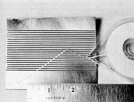
FIGURE 8: Unfinished Etched Printed Circuit Board for Adapter.
MAKING A CUSTOM CONNECTOR
There are 40 contacts on the cartridge port, 20 on each side of the edge connector. A blank piece of double-sided printed-circuit-board material, approximately three by five inches in size, was cleaned thoroughly with extra fine steel wool, then washed and dried. (For both sides of the final product to align properly, one of the longer edges of the board should be quite straight and used as a reference.) Both sides are marked at each end with sets of 20 points at 2 mm intervals, starting approximately 1/2 inch from the reference edge. Strips of thin adhesive tape are then placed on each side of the board, positioned carefully using the marks as reference. (The tape I used, the type used by draftsmen and illustrators for graph and chart production, was 1/64 inch wide. Thin, printed-circuit artwork tape could also be used.) Care should be exercised to ensure the tape is straight and tightly stuck down. Both sides of the board are then lightly but completely sprayed with acrylic enamel and permitted to dry. (A slightly warm oven could be used to hasten the process.) Following drying, remove the tape, exposing the copper beneath.
The board can now be etched in the standard manner, leaving a set of 20 parallel traces in correct alignment on each side of the board (see Figure 8 ). A section of the board about one inch long is cut off and finished according to the dimensions in Figure 9. It is recommended that the copper at the extreme edges, particularly on the narrower section, be removed to prevent peeling and possible electrical interference in the cartridge connector. The bevel shown must be made on the edge to be inserted into the cartridge slot, otherwise it is possible to snag one of the fingers in the cartridge port and push it down into the opening where it will short to the finger on the opposite side. (The short will not disappear when the board is removed, the machine will not operate correctly, and you will have no idea of the cause.)
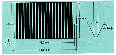
FIGURE 9: Finishing Dimentions for Adapter Card.
The semi-finished board should then be cleaned carefully with solvent or steel wool. It is important to remove all traces of the enamel to facilitate soldering to the copper. A piece of 40-conductor ribbon cable, between six and eight inches long, is prepared as. follows. After ensuring the ends are cut squarely, a line is drawn across the cable about three quarters of an inch from one end. Carefully, the conductors are separated back to the line. (A sharp knife, scalpel, or scissors can be used to cut back 1/8 inch between conductors, then the wire can be torn back by hand.) 1/8 inch of the insulation is stripped from the ends of the separated wires and they are then tinned with solder. The ribbon is placed on a flat surface and the odd-numbered wires are pulled to a vertical position. (The first wire, usually indicated by a colored stripe on the edge of the ribbon, must be upward.) These conductors will be soldered to the top of the edge connector, the even-numbered ones to the bottom.
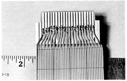
FIGURE 10: Photograph of Ribbon Adapter Assembly.
The middle two wires in the ribbon for the top surface are soldered to the matching conductors on the board as are those for the bottom, ensuring no slack is left in the wires. Then, alternately, wires on either side of the board are soldered until the outside conductors are done last (see Figure 10). This way all possible slack can be eliminated from the wires and equal stress can be applied to all regions of the board when pulling on the ribbon to remove the connector from the Atari. (Prepare and count carefully! It is most embarrasing to have one wire left over when you are done.)
When the edge connector is finished and inspected, the header matching the one on the interface card can be mounted. It is suggested that this be done after the edge connector is soldered in case the ribbon is damaged and a new start must be made. Conductor #1 should be oriented correctly in the header (usually indicated by a small arrow-head in the plastic) and the connector crimped home using the correct tools or a small vise. The maximum length of about eight inches for the adapter ribbon ensures little effect on the bus signals. Extending it might cause crosstalk among the conductors, leading to irregular operation of the system.
The ribbon should be made as short as possible, remembering that the interface rests on the work surface to the left of the computer console. The builder might consider folding the cable at a right angle to place the interface to the rear of the computer. This will, of course, invert the numbering on the interface connector and care must be taken in wiring and documentation. It is worthwhile to remember that the odd-numbered contacts on the cartridge connector are on the top.
BLUE-SKY DEPARTMENT
The control signals passed to and received from the external hardware might be either low- or high-true. To accomodate this, two inverters, IC7A and IC7B could be provided to condition the inputs, and either output polarity from the data-available latches (IC3A and IC3B) might be selected as indicated on the schematic by the jumpers JP1 thru JP4. For the implementation done here, the input lines did not require conditioning so IC7 was not required. (Both 1C3 and IC6 clock on the rising edge of the strobe pulse, ISTB, but the external hardware provided a low-true pulse. Thus the data and status were not available to the ST until approximately one microsecond after the external device had actually provided it. The inverter IC7A should have been implemented to eliminate this delay, but in the worst case, loading 184K bytes of image data, the aggregate time lost amounts to only two-tenths of a second in a 12-second transfer. For implementations requiring higher rates, these types of considerations should be weighed carefully.)
An additional seven output bits can be made available simply by adding a 74LS374 data latch to the high-order (A15-A9) address bus. The output latches should be clocked together. Should some minor address decoding be required, to implement further input and/or output ports, qualification of -ROM3 and -ROM4 with a high order address bit (A15 typically) can be done using three-input or cascaded two-input gates.
This interface foundation could be the basis of any number of other, real-world sensor/controller combinations. The outputs can be implemented with relays or opto-isolators for controlling external devices, while analog to digital (A/D) converters could be connected to the inputs for medium-speed data acquisition.
REFERENCE:
* ATARI ST internals, The Authoritative Insider's Guide by K. Gerits, L. Englisch and R. Bruckmann, Abacus Software, Grand Rapids, MI
LIST OF MANUFACTURERS:
* Cartridge Prototype Board
Bigfoot Systems, suite #207
2708 E Lake Street
Minneapolis, MN 55406
(612) 722-9515
CIRCLE 428 ON READER SERVICE CARD
* NEXUS OMNEPROM
(EPROM development system)
NEXUS Technical Services, LTD.
38 Melrose Avenue
Reading RG6 2BN
England
(0734) 664559
CIRCLE 429 ON READER SERVICE CARD