A 16-BIT CARTRIDGE PORT INTERFACE
BY RANDY CONSTAN
On the side of your Atari ST lies one of its most powerful hidden features: the cartridge port! Through this subtle interface lies the potential for an incredible array of untapped resources. Consider 15 address lines, 16 data lines and four control lines are brought out. Any device connected to the cartridge port can be directly controlled by the mighty 68000 processor with no "middle man." Theoretically, over 256K bytes/second could easily be transferred. With the proper circuitry, over one million discrete processes could be individually monitored and controlled through this port. And, with the proper software added, an entire robot-controlled assembly line could be run entirely with the ST!
Consider our problem: One of my current projects involves the design of a new electronic musical instrument. The sounds produced by the instrument, however, won't be new at all; they will be "sampled" sound. Sampling is a technique in which a sound wave is converted into numeric computer data, which can later be reconstructed into sound. If you've heard a CD recording through a quality stereo system recently, you know what the state of the art in this technology sounds like. Making a CD-quality recording, however, is no easy task. It involves doing over 40,000 analog-to-digital conversions per second, each to an accuracy of 16 bits. Several articles could easily be written on this subject alone, but whatever circuitry is used, the questions of speed, memory and control immediately come to mind. How can we precisely control the timing of these critical devices and instantly save the hundreds of thousands of data words that are pouring in at a rate of 44,000 per second?
|
Warning: The following article is for ST owners with a large amount of electronics experience. If you lack this experience, do not attempt to build this project for use with your SI You may damage your computer. |
ST to the Rescue
A general-purpose interface device for the ST was in order. The 68000 processor easily surpassed the speed and memory requirements, and the cartridge port provides neat and eloquent access to this power. In this article, we'll discuss the design and construction of a versatile cartridge-port interface, which will provide 16-bit, latched data, read-and-write capability, complete with status and handshaking control. Before you go running for your soldering iron, however, a word of warning. Building this interface does require a lot of tight wiring on a relatively small circuit board. Wiring errors, aside from causing a great deal of frustration, could damage your ST. I have found that the cartridge port will tolerate some momentary shorting of address, data and control busses, and even an occasional power-supply short, with seldom more than a system crash as a result. But don't count on it! Be very careful wiring and rechecking. Let's just say that if you're contemplating this as your first electronic project, skip over this article!
Cartridge Basics
All 16 data lines and address lines, A1 through A15, are brought out to the ST cartridge port. Since the 68000 can address two bytes (16 bits) of data at a time, there is no address bit zero. Instead, two control signals, UDS (upper data strobe) and LDS (lower data strobe), are present. When the processor wants a word (16 bits) of data, the proper address is asserted on the address lines and both UDS and LDS are simultaneously brought low (Logic 0). If only a single byte (eight bits) is desired, the same process occurs except that only one of these signals will be strobed: UDS for even bytes, and LDS for odd. So, it is possible to create an A0 address line using UDS and LDS. Moreover, it is possible to have several different operations based on the various combinations of these signals.
With 16 address lines, we could address up to 64K in our circuits. The 68000 actually has 24 address lines however, and can address up to 16 megabytes! So the ST cartridge port has two more control signals available, and our circuit will know when the port, and not some other 64K bank of memory is being addressed. These are ROM3 and ROM4. Rather than bring out all 24 address lines, two possible 64K cartridge-bank address ranges are sensed by the ST's "glue" chip. When any address in the range of $FB0000 through $FBFFFF is asserted, ROM3 is strobed to logic zero. The other cartridge bank occupies the range of $FA0000 through $FAFFFF, and any address in this range will cause the ROM4 control line to be strobed. Note that numerically, it would seem as if this were an error. However, the text is indeed correct: ROM4 is for the lower $FAxxxx range and ROM3 for $FBxxxx. So, by using these control lines, we can easily prevent our interface circuit from interfering with any other memory operation that does not involve the port.
Now for another "zinger." Since the cartridge port was originally intended to (you guessed it!) read cartridges which are normally just ROMs, Atari in its wisdom saved a few bucks by making the data lines (D0 through D15) unidirectional. In other words, data can be read in, but not written out on these lines. Since we want to be able to transfer data in both directions through our interface, we need to overcome this problem. Notice though, that the address lines have the exact opposite property: Data ("address" data, that is) can only be written out of the port. So if, for example, we wanted to write the word $E812 through the port, we could make our circuitry respond to the ROM4 address range, and simply do:
def seg = &hfa0000
a = peek (&hE812)
in BASIC, or:
move.b $FAE812, d0
in assembly.
What we've done here is fool the system. The ST thinks we're reading a byte from location $FAE812, but what's actually happening is that the lower portion of the address data is being written to the port. (Note that the data returned is irrelevant.) So, since we have two memory-bank control lines available (ROM3 and ROM4), I decided to simply make two independent 16-bit interfaces on the one board: one for reading data, the other for writing. Also, the UDS and LDS control lines are used to provide a "get status" function, in addition to read and write.
The Interface Circuit
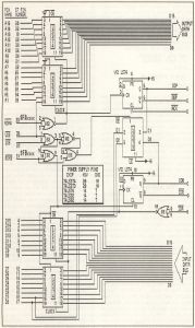
Take a look at the schematic in Figure 2. The two upper 74LS374 chips each contain an 8-bit latch. Whatever data is present on the latch inputs will be saved when Pin 11 goes high, and will remain available for output until Pin 11 cycles low and high again. At this point the new data will replace the old. All 15 available address pins (A1 through A15) are connected to these inputs, and since one more bit is desired (A0), UDS is connected as well.
The control pins, UDS, LDS, ROM4 and ROM3 are all active low. This means that they normally sit high (+5 volts) until activated, when they momentarily become low (0 volts). The ROM4 line is inverted and passed to Pin 11 of both chips, so that addressing the $FAxxxx range will cause the lower 16 bits of address to be latched. As it turns out, the ROM control lines change last, after the address, data and UDS/LDS, making them perfect for this critical timing.
In our previous example, the bit pattern corresponding to $E812 would now be available at the output of our interface and would remain available indefinitely. The inverted ROM4 signal is also used to set a flip-flop, which can be read by the ST or an external device as an output data pending (ODP) signal. This flip-flop can also be reset by an external device by pulling the acknowledge (ACK) line low. The point here is to accomplish "handshaking." An external device such as a D/A converter can be set up to wait for the ODP signal before accepting new data, and after the data has been transferred, can cause the flip-flop to reset. In the meantime, a software loop can poll this flip-flop, until reset has occurred, then send new data to the port.
The read logic works in a somewhat reverse fashion. In this case, an external device such as an A/D converter (or another ST!) would place data on the 16 INPUTs provided. Then, the device would have to momentarily pull input data available (IDA) low. This would latch the data into two more LS374 chips, and set the IDR (input data ready) flip-flop. Again, a software loop polling the flip-flop would determine that IDR has been set, so it would "know" when it's time to read the data. This flip-flop will automatically be reset by the read, so that the external device will know it's time to send more.
Now here things get a bit tricky (bear with me!). Note that the LS374 chips are connected directly to the data lines. Any data continuously impressed on these lines would cause the ST to lock up almost instantly. We must have a way of making this data appear to be totally disconnected from the data bus until the very moment we need to read it. To accomplish this, the LS374 chips have a pin called output enable (OE). When this pin is brought low, the latched data will be present on the output. When high, however, the output pins become transparent (high impedance), so that no bus interference can occur. By setting up our logic so that any word size read from the $FBxxxx range triggers the OE pin, we can read in the latched data at a convenient time without the worry of bus interference.
Finally, a Status function has been provided to complete the handshaking system. Recall that reading a word from the $FBxxxx area will result in reading the latched external data and clearing the IDA flip-flop. If, however, an odd byte is read from the $FBxxxx range, the Q outputs of both flip-flops will be read into D0 and D1, without clearing either one. This is accomplished by activating the OE pin of the LS373 during a "byte" operation.
Construction
So, enough talk—let's get busy! The first thing we'll need is an electronic prototype board, with pin spacing to accommodate the 40-pin port.
Until recently, you would have to build and etch this board from scratch. Now however, there are at least a few vendors for this item. I obtained some very nicely constructed boards for only $10 each from Douglas Electronics Inc. in California. (See Figure 1 and the address in the parts list.)
Second, you'll need the eight ICs shown in the parts list, together with three 14-pin and five 20-pin wire-wrap sockets. A 40-pin termination header is also required on both the internal and external side of the interface board to facilitate connections and testing. Finally, you'll also need at least three 0.1 microfarad, ceramic disk capacitors to be connected across the power supply rails at various points on the board.
The IC sockets, termination headers and capacitors can all be obtained at your local Radio Shack store. For the ICs however, you may have to shop around at an electronic specialty shop. Also if you've never done wire wrapping before, now is a good time to start. While I did quite a bit of point-to-point soldering on my prototype, I found the process to be quite troublesome. The connections are so close to each other that hairline solder bridges between soldered points are almost inevitable. If I had it to do over, I would have wire wrapped the entire project.
Figure 2 shows both sides of my completed board. The plastic cover on the "wired" side helps protect the unit, and helps it to stay nearly level when plugged into the port. The board layout is by no means critical, so feel free to use your own judgment here. I do suggest that you obtain at least three colors of wrap wire, so that output data, input data and steering-logic wiring can be more easily distinguished.
The Douglas board already has several supply and ground conductors etched on the board, so that power-supply wiring to each chip requires a minimum of effort. The supply lines to your wire-wrap IC sockets, the three capacitors, and the pin headers will have to be carefully soldered in. The internal (ST) side header must be soldered with the pins facing down, since that's where all the wiring will be done.
The rest of the project can then be completed exclusively with wire wrapping. With the prototype board face up (the side with the manufacturer's name), Pin 1 is the at the top rear of the board as shown in Figure 1. You can refer to your ST owner's manual (page 77) for identification of all the cartridge port pins. These are also listed on the left side of the schematic.
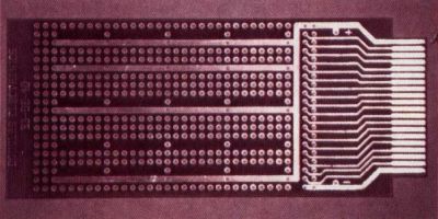
The Douglas prototype board. Pin I is marked for reference.
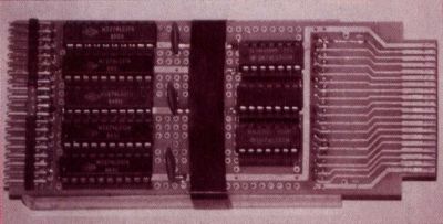
The completed cartridge port interface. Note that component layout is not critical.
Carefully solder in the IC sockets (supply pins only), along with the headers and capacitors. The small chart in the center of the schematic shows the power pin locations for all the ICs used. Check the wiring with a multimeter until you're sure no shorts or wiring errors are present. Power supply errors are among the most unforgiving, so be forewarned!
When this step is completed, proceed with the rest of the wiring. Again, no special layout is required, but remember that neatness goes a long way in avoiding headaches when the time comes for correcting errors or modifying the circuit. It would also be advisable to draw a map showing how you intend to wire the external side pin header. As a final step, connect two eight-inch lengths of insulated, flexible wire to a convenient ground (zero volts) on the board, and strip off no more than ⅛ inch of insulation at the unconnected ends. These will be used for testing the interface.
Testing the Unit
The first test of the unit should be done with none of the ICs plugged in! Carefully plug the board into the cartridge port, and power up the ST with a formatted, but blank, disk. If you don't see the desktop come up within a few seconds, turn off the power immediately and re-check your wiring. Again, an inexpensive multimeter is helpful in determining whether address/data lines have been shorted. Since no chips have been inserted, infinite resistance should be present across any pair of these pins. If the desktop comes up normally, check for power on all the IC sockets.
Next, power down the ST, remove the interface and insert the ICs into their proper locations. Repeat the above "smoke test" to make sure the desktop appears with the complete interface inserted. If all goes well, it's time to test the unit for proper operation under software control.
Connect one of the temporary ground leads to the negative test probe of a multimeter and set the meter to measure five volts. Then, power up the computer and boot-up good ol' ST BASIC. All right, I know, I shouldn't have used the word "good," but for simplicity's sake, it would be nice if we could use the port from BASIC. We've already seen how we can test the Write operation. In direct mode (command mode), type:
def seg = &HFA0000
This does two things. First, it sets the base memory location for future peeks and pokes. Second, when DEF SEG is equal to anything above zero, it causes all peeks and pokes to return a byte value.
Now type:
a = peek(0)
Next, using the positive probe of the voltmeter, check that all 16 data outputs on the interface are at near zero volts. Then, type:
a = peek(65535)
Using the same procedure, you should now find that all the data output terminals are at approximately five volts. If this does not work as expected, you still have some wire checking to do! By peeking the number 65535, we have effectively written a binary 1111111111111111 on the address bus, and so all outputs should be high. Now recall that the second ROM bank (ROM3) in the cartridge address space is used for reading data in our interface design. But, here there is a serious problem! Unfortunately, when BASIC performs a PEEK (or POKE), only one byte at a time is addressed. This is true even though a BASIC PEEK command will return a two-byte number if DEF SEG = 0. BASIC simply peeks two bytes, one at a time.
There's no easy way to test the Read command of our interface, since the byte-oriented BASIC will never cause UDS and LDS to simultaneously strobe. Arrrgghh! Then I discovered the Call command which allows BASIC to access a machine-language program. (Special thanks to Charlie Bachand for showing me that the Call command is much simpler to use than the manual would have us believe!)
So if you've gotten this far, boot-up BASIC, type in Listing 1 and save a copy on disk. This short program uses a machine-language patch that allows the Write, Read and Status functions to be tested and will make our experimentation a whole lot easier. For those interested, the source code for the patch is given in Listing 2, which you need not type in.
When the program is run, a short menu is displayed with the options Write, Read and Status. For starters, let's repeat our last experiment. Select Item 1 (Write) and press Return. The program will prompt you for the data you wish to write. Type 0, press Return and once again check that all data outputs are zero volts. Then, press Return to resume and select Item 1 again. This time, enter FFFF (all entries in hex!) and observe that all data outputs are at five volts.
Next, select Item 3 (Status). The IDR and ODP flags will be read from the interface and displayed. The IDR flag is undefined right now since no data has yet been read from the port, but the ODP flag should indicate "SET"
Now, using the other temporary lead, momentarily ground the ACKnowledge pin on the interface, being careful not to touch anything else with the wire. Repeat the Status function, and ODP should be "CLEAR."
Now, let's test the Read function. Momentarily touch the IDA terminal with the ground wire, and again select Item 3. IDR should now definitely be "SET" Next, select Item 2, and the port data will be displayed. It should be $FFFF since all data input pins were unconnected when you strobed IDA. Remember that with TTL logic chips, an open connection is always considered logic Level 1. Selecting the Status function now shows that IDR has been CLEARed by the read function.
Now the next step is a bit tricky. Disconnect the first temporary lead from the multimeter, so that you have two "ground" probes free. With the first probe, touch the D0 pin on the input data bus, and while holding this wire in place, carefully touch IDA with the second. Now, put down the leads, select Item 2, and the data read should be $FFFE. This procedure will allow you to test all 16 data inputs by verifying that the hex data matches the pin you grounded when IDA is strobed. To help reduce this to a "two hands" operation, you can temporarily add the following line to the BASIC program:
735 goto 720
This will cause menu Item 2 to continuously read and print the port data, so you can keep testing with the ground probes while you keep your eye on the screen. Testing the output data leads is much easier, since you need only select Item 1 to write data and use the multimeter to check the results.
Suggestions for Further Development
Obviously, to gain maximum speed advantage from our interface, assembly language is needed. You can use Listing 2 as a guide, but note that the code must be executed in 68000 supervisory mode. Since BASIC does this for us when the CALL command is used, this listing does not include this task. Also, for maximum speed, it is possible to disable all interrupts by setting the IPL in the 68000 status register to seven.
To use the system from BASIC, all that is really needed are lines 100 through 190, and 1000 through 1040. Then, poke the variable command with one, two or three for the functions Write, Read and Status, respectively. For the write function, poke cdata with the 16-bit integer you want to write to the port. Finally, enter CALL CARTPORT
For Read and Status commands, the data returned can be obtained by peeking cdata. Never poke the cartridge address range, as this will cause a bus error and crash the system. Let the CALL function do the work, and you'll always be safe.
On the hardware side, there are many additions and modifications possible. For example, wiring in the six unused bits on the 74LS373 chip will enable the Status function to monitor six more external inputs. If this is done, you'll have to change the &h0003 to &h00ff in line 1040 of Listing 1, to allow eight bits to be monitored by the Status function. Also, if handshaking is not needed, LS373 chips can be substituted for the LS374s in the data input section. This way, strobing the IDA pin will not be necessary.
It is also possible to create more functions by adding steering logic to sense word-size access of the ROM4 address range. This, as well as "even byte" access of ROM3, has not been utilized. My only caution here is that you should not make any ST side signal drive more than two or three TTL gates without some kind of buffering.
As far as application goes, the list is endless. Instant data transfers between two STs, PROM burners, data acquisition and supervisory systems are all possible. Don't be afraid to experiment! And, drop me EMAIL if you come up with anything interesting (CompuServe: 73637,317).
PARTS LIST
| Item | Quantity | Possible Source |
| 74LS374 | 4 | Local electronic distributor |
| 74LS373 | 1 | Local electronic distributor |
| 74LS74 | 1 | Radio Shack |
| 74LS32 | 1 | Radio Shack |
| 74LS02 | 1 | Radio Shack |
| 40-pin headers | 2 | Radio Shack |
| Prototype board | 1 | Douglas Electronics 718 Marina Blvd, San Leandro, CA 94577 |
It is possible to create more functions by adding steering logic to sense word-sized access of the ROM4 address range.