FEATURE TUTORIAL
Step 1
THE HARD FACTS
A look under the hood—part 1
by Maurice Molyneaux
Allergic to all things Commodore, Maurice Molyneaux is an author and artist, who—when not writing articles for ST-Log—continues to struggle with a recalcitrant 8-year-old science fiction novel, paints, illustrates and also uses his ST for "every conceivable task." His interests include classic cel animation as well as the computer variety, and he draws the meanest Star Trek pictures on microcomputers. His Delphi username is MAUR1CEM.
Thus far, Step 1 has been geared to explaining the ST systems in a manner intended solely to give the beginning user some idea of what the system is capable of doing, and how to use it. I certainly intend to stay in that vein, but this month we're going to take a detour from the norm and briefly tour the ST hardware...and I don't mean a description of the ports, etc., as appeared in the very first Step 1. This time we're going to go deeper...into the very bowels of the beast. Next month, when we continue this discussion, we'll go into further detail.
Before you beginners cast this aside, feeling I've betrayed you and am pandering to techies, hang on. There are reasons for covering this subject. First, many ST owners ask why their machines can't do this or that, not knowing a lot of the reasons are in the hardware. Second, things can go wrong with a system. If you know something about the hardware and how it works, it's easier to fix simple problems on your own, or tell a technician exactly what's wrong. For those of you interested in a "How-NOT-To" lesson on computer repair, read Matthew Ratcliff's "ST Nightmare Repair" (ST-Log issue 12), and learn from his mistakes. Third, it's not a bad idea to understand just how a computer works, because then you can better appreciate its strengths and limitations.
Finally, I don't want a bunch of letters from techies castigating me for my brief—and rather nontechnical—descriptions. This article is meant to give the average user some idea of what goes on inside his or her computer. It's not a detailed analysis of ST architecture.
The grand tour
Now, we're going to pop the hood of a 520ST, and take a look around. 1040ST and 520STfm owners can rest assured that everything described here is the same in their machines, though the exact placement of parts may differ. For this tour, there's no need to open up your ST, as that will void your warranty (if it's still in effect). Photographs are provided to show you what I'm talking about.
Under the ST's pretty gray top is the keyboard. The keyboard is not attached to the top part of the system case, but sits on supports in the lower half. On the bottom of the keyboard are a cluster of electronic components and a chip ("chip" is the nickname for an "Integrated Circuit" or "IC"). The chip is a small processor IKBD or Intelligent KeyBoarD controller. It provides the main processor (the brain) of the ST with information related to the state of the keyboard, real-time clock, mouse and/or joysticks.
One feature of this chip is that it contains the real-time—or time of day—clock (set from the control panel accessory). The time and date set in this clock are "stamped" on a file entry when you save it to disk. If you always display directories on the desktop using icons, select "Show As Text" under the view menu, then open a directory window. If you can't see the date and time, resize the window horizontally or click on the "full screen" button in the window's upper right corner. Now you should see that each filename has next to it its size in bytes, in addition to the date and time it was saved.
The clock in the IKBD, and every other component, loses all power when you turn off your ST, so the time and date settings are lost—unless you have a Mega ST, or have added a battery backup clock to your system. On system power-up, the clock is set to a default time and date, which can be changed from the control panel. If you aren't in the habit of setting the clock, don't expect the correct time and date to be stamped on your files.
The IKBD's main functions are monitoring the keyboard and the mouse/joystick ports. Whenever you use the mouse, fiddle with a joystick, or press a key on the keyboard, the action is noted by the IKBD, which passes the information deeper down into the system.
The IKBD is a chip manufactured only for Atari ST systems. Such specialized parts are called "custom" chips because they're custom built for a given system. Other chips are considered "off-the-shelf" because they can usually be purchased at an electronics store. If you need to replace a custom chip, you'll have to contact Atari or an ST service center. In this article, all custom chips will be indicated as such. All others are off-the-shelf.
The keyboard is connected to the depths of the ST by a tangle of colored wires, which descend through an opening in the metal shield below the keyboard, and are fitted into a slim connector. The connector must be pulled up and out in order to go deeper into the system.
Now that we've done that, we're faced with a big sheet of dull silver metal. This is the ST's RF shielding. RF stands for Radio Frequency, and shielding means what the name implies, only twofold. This shielding prevents outside radio signals (radio, TV, etc.) from interfering with your computer's operation, and vice versa. This shielding isn't a complimentary feature—the FCC (Federal Communications Commission) is very serious about radio interference.
The shield consists of two halves, top and bottom. To look inside, we must remove a few screws, then untwist a bunch of metal tabs—one or more of which may be soldered down. Once this is taken care of, we can lift the top portion of the shield and...Behold! Here is the heart of the ST . Not much to look at, but this is what makes it work.
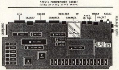
Under all the pretty gray plastic and white keys we find a printed circuit board: A big flat panel, covered with electronic gizmos, sprinkled with black chips, and rimmed with port connectors. (There's also a power supply and floppy drive in the 1040ST, 520STfm and Mega ST, as well as a fan in the Mega). This board is the center of the entire computer system. Because it's the main component, it's called a "motherboard." Consequently, add-on boards are called "daughterboards," since they spring from the motherboard.
Here's where we stop and look around. I'm going to briefly introduce you to the parts of the system that make your ST an ST, and not a C-64 (shudder).
All parts are labeled with letters, so the following descriptions will correspond with the marked components.
Before we begin the tour, let me explain the difference between serial and parallel interfaces, as some parts will feature these. A serial interface is one in which data can travel in only one direction at a time, one bit at a time. A parallel interface is one where data is transferred a byte at a time, by sending all 8-bits simultaneously, in parallel, a number at a time—side by side, so to speak. The MIDI and modem ports of your ST are serial interfaces, while the printer port is a high-speed paralle interface.
The big brain
A — This is the biggest and most important chip in the ST. It's the brain and heart of the entire system: the microprocessor. A microprocessor receives data, processes it, then outputs data and instructions for other parts of the computer system. The ST's microprocessor is a Motorola MC68000. The 68000 is a fast and powerful 16-bit microprocessor. When we refer to bits, we're referring to the number of data bits (on/off signals) the processor can handle at any given instant. The 68000 can handle 16 data bits at a time (cycle). The 6502 processor used in Atari's 400, 800, XL and XE models can only handle 8 bits of data each cycle. This means that with each processor cycle, the 68000 can process twice the number of bits a 6502 or other 8-bit processor can.
Different microprocessors, and various versions of the same models, have different "clock speeds," which refers to the number of cycles per second. The Atari 8-bits’ 6502 has a clock speed of 1.79 MHz (1.79 million cycles per second), while the ST's 68000 runs at a dazzling 8 MHz (8 million cycles per second!). This means the 68000 runs nearly 4.5 times faster than the 6502, and can address twice the number of data bits per cycle.
So, in raw processing terms, the 68000 can handle close to 9 times more data per second than the 6502! Of course, this doesn't mean an ST is 9 times as fast as an Atari 8-bit, because there are a lot of other factors that contribute to overall performance. For example, the 68000 is a 16-bit chip, but many of its peripheral ICs are 8-bit, and cannot move data as quickly as the 68000. Further, some chips "hog" the address and data buses (buses are accesses to RAM addressing and data lines) and keep the 68000 from using them. This is called "cycle stealing," and chips that do this can slow down overall speed when they are in use. Therefore, clock speed alone doesn't mean a whole heck of a lot. If nothing else, you should now have a better idea of how the brain compares to that of the older 8-bit systems. (I'm not knocking them, honest!)
While the 68000 has a 16-bit data bus, its address bus is 24 bits wide. Internally (inside the chip), its own data and address registers are 32 bits wide. (Registers are places where the chip stores values.)
There are eight data and nine address registers in the 68000. I won't go into what this means, but I can tell you that this is the reason the 68000 is often referred to as a 16/32-bit microprocessor. And, if you've ever wondered just what "ST" stands for, it refers to the Sixteen/Thirty-two-bit processor. Because of this design, the 68000 can directly address up to 16 megabytes (16.384K!) of memory. Conversely, the 8-bit 6502 can directly address only 64K! To use more than this, a 6502 must "switch" between different banks of memory (as does the 130XE).
Finally, note that the 68000 is soldered directly to the ST's motherboard. This is called "surface mounting" and is usually carried out only on parts with high reliability and very little chance of failure. Sometimes, though, parts are surface mounted to keep costs down, in addition to improving reliability, because a soldered down part can't come loose.
Many other chips are set in sockets, which means their pins (legs) are pushed into a special receptacle. Socketed chips can be popped out with little effort. Although more expensive than surface mounting, socketed chips are much easier to replace if damaged, or if an upgraded chip becomes available. I will denote the status of each chip in its description, but please keep in mind that variations do occur, and I cannot speak for parts in the Mega, as I haven't yet seen the guts of a production model. The IKBD chip, discussed earlier, is socketed.
Pardon the interruption...
B—The handling of interrupts is a crucial part of any computer system based on a 68000. In the Atari, this is accomplished through the use of a Motorola 68901, also known as the Multi-Function Peripheral (MFP) chip. It's called "multi-function" for good reason: it handles quite a number of tasks. Its primary job, however, is handling system interrupts. For example, in some systems, the processor monitors things like the keyboard and joyports a number of times each second. This uses valuable processor cycles, which could be better utilized in doing calculations, etc.
In a 68000-based computer, the MFP stands in "front" of the 68000, intercepts all interruptions from other parts of the system, carries out various interrupt control measures, then passes them on to the 68000. In this way, the 68000 merrily goes about its business, not having to monitor other parts of the system. When something requires the 68000's attention, the MFP sort of "taps the processor's shoulder" and makes it aware of the event. In other words, an interruption.
The MFP's job entails more than that. Its features include an 8-bit parallel port, a built-in serial interface and the ability to handle 16 possible interrupt sources. Further, the chip contains four timers. One of these, the 200-Hz clock, is used for all of GEM's timing. The chip itself runs at a 4-MHz clock speed. The MFP chip is surface mounted, and not easily replaced.
ROM wasn't built in a day
C—This bank of six chips is the ST's ROM, containing all the code for TOS and GEM. These chips, more than anything else, are responsible for making your ST work the way it does. These chips are socketed, and can be easily replaced if need be. The total ROM of all the chips combined adds up to 192K. Because they contain the ST's OS (Operating System), they are, of course, custom chips.
Sticky stuff
D—This is the system's electronic "adhesive." The chip serves to interface various components and works the peripheral chips. Due to its importance in holding everything together, this chip is aptly named Glue (also GLU, for General Logic Unit). Glue communicates with just about every component in the ST, and keeps watch over all operations.
In many other systems, a complex array of smaller parts handle the functions of Glue. Because of this, it's difficult to briefly describe just what Glue does. Since Atari consolidated all these functions into a single chip, the cost of manufacturing the computer is kept down, which helps make it as affordable as it is. Glue is seated in a 64-pin socket, and often held in place by a metal clamp. It's a custom IC.
I remember!
E—This is the ST's Memory Management Unit, or MMU.
The MMU's primary job is to interface the processor with the system's RAM (memory). It also works with the system's video chip to produce the video signal for your monitor—giving it access to the RAM which contains the data for the screen. Further, the MMU works in conjunction with the system's DMA chip, for passing data between RAM and the DMA/hard disk and floppy disk ports.
This chip handles "who gets what RAM and when," thus keeping your desk accessories and Neo-Chrome from trying to simultaneously occupy the same RAM. It is primarily the MMU that limits current ST systems to addressing only 4 megabytes of RAM, although the 68000 is capable of addressing up to 16 megabytes. MMU runs at a blinding 16-MHz clock speed. Like Glue, it is a custom chip, is seated in a 64-pin socket, and usually held in place by a small metal clamp.
Quick and direct
F—This is the ST's DMA, or Direct Memory Access chip. Its job is to oversee the floppy disk controller chip and the hard disk—or anything else plugged in through that port, like a CD-ROM or IBM emulation box. This chip is tied into the processor's data bus, allowing very fast data handling. DMA can eliminate the need for data to be moved through the 68000 when it's being transferred between a peripheral device and the ST's memory.
When dealing with the floppy drives, the data transfer rate is so slow that the 68000 has no trouble dealing with direct transfers. However, because the DMA/hard disk port has the potential to move data at a rate of 8 megabits per second (no device, at this time, uses this port at that speed), this could cause severe problems for the 68000! In fact, when dealing with a hard disk or other high-speed device, the 68000 uses the DMA chip to send "pause" commands to the device, so it will wait while the 68000 processes the data it has.
The DMA chip—because it works with both floppy and hard disk interfaces—is a likely source of trouble if you begin having problems with one or both. I recently had hard disk and floppy access problems, which were partially due to a bad DMA chip. Fortunately, this chip is socketed, and easily replaced. DMA is a custom chip.
The wild, wild west
G—This chip is a Western Digital 1772, a component with one task: control the system's floppy drives. This chip features built-in drive motor controls, and supports single-and double-density formats. Atari chose this chip, despite its limitation of being able to use only two floppy drives, because it offered a complete floppy controller in a single chip. The WD1772 is socketed.
Sounds complicated
H—This chip is a prime example of Atari's attempt to maximize the effectiveness of each component of the ST system and keep the cost down. The chip, a Yamaha YM-2149 PSG (Programmable Sound Generator), not only serves the task of adding audio to your ST's video, but it also features two bi-directional 8-bit parallel ports.
Atari chose the YM-2149, not only because it was an inexpensive and reliable sound chip, but because they also got those parallel interfaces in the bargain. This reduces the number of overall parts, as this chip handles both sound and the printer port. The same component is also made by General Instruments, and called the AY-3-8910.
The YM-2149 can generate sounds on three separate sound channels, over a range of between 30 Hz and 125 KHz. The chip also features a noise generator for distortion. While not as capable as a custom sound chip would be, the YM-2149 does provide decent sound. Atari has hinted of a super sound chip called AMY, but whether she will ever emerge from the vapor is doubtful.
In many STs, the YM-2149 is surface mounted, but on the Revision H motherboard I recently obtained, it was socketed. If you have problems with your printer port, this chip could be to blame.
Keys and music
I—Here, we have a rare case of two identical components, a pair of 6850 ACIAs. ACIA stands for "Asynchronous Communications Interface Adapter." The ACIAs are serial interface operators and, while identical, each of the two chips has a special job. One chip is interfaced to the IKBD and, therefore, communicates with the keyboard, mouse/joystick ports, and runs the real-time clock. The second one controls the (serial) MIDI interface.
Many people do not realize that, while the MIDI ports are primarily intended for use with electronic musical devices, they are serial data ports. Thus, they can also be used to network other types of hardware together. The MIDI-Maze game by Hybrid Arts uses the MIDI interface to connect multiple STs together for a round of game action. These two chips are surface mounted.
You look mah-velous
J—This chip is concealed under a small RF shielding box on the motherboard, and is surrounded by video circuitry. This is the video chip, called Shifter, which converts screen information in RAM to signals necessary for a monitor. The 520STm, 520STfm and 1040STfm models (which feature TV output) have additional circuitry for an RF modulator (which converts the video signals into those used by a television). When such a modulator is present, additional pins are connected on the ST's monitor jack, providing a composite video signal—which is what's utilized by monitors used with Atari 8-bits, etc. The composite signal is not available on STs without an RF modulator.
Shifter contains 16 "palette registers," which hold the values for the colors you use when in color mode. Only four of the registers are used when in medium resolution, but all 16 are used in low resolution. If you wonder why your ST is normally limited to only 16 colors at a time, look no farther than Shifter.
Note that Shifter is a socketed chip. In many cases, RAM expansion boards for the ST will plug into the Shifter socket in order to gain access to RAM address lines. A bad or poorly seated Shifter chip is often the root of problems relating to screen display. Distortion or garbled images are often signs of a problematic or loose Shifter. Shifter is a custom IC.
K—This is the RF modulator, present in all 520STs manufactured after 1985, and a tiny handful of 1040STfms released last summer. The shielded box here contains the RF signal converter, and a channel select switch for choosing which TV station you'll be using. To add such a unit to an ST can be complex, because usually the associated video circuitry for RF is missing.
Pretty chips all in a row
L—This row is very important. The 16 chips here (32 in a 1040ST) are the system's RAM. This is the memory where all the important information (like text, graphics, etc.) are stored and manipulated. These chips are known as 256×lK chips, and 16 of them provide 512K of RAM, while 32 provide 1024K (1 megabyte). In a Mega ST4, there are 16 1-megabit RAM chips, providing 4 megabytes of memory. These chips are surface mounted, and there's no simple interface for plugging in additional RAM (though the processor bus in the Megas might change this).
Fast mover
No identifying letters here. You won't find this part in your 520 or 1040, but you Mega owners will. In the Mega ST there's an IC that we've been waiting on for a long time: the Blitter chip. The Blitter is a custom microprocessor whose primary task is moving blocks of memory at high speed. STs without a Blitter chip accomplish their blitting (a method of moving blocks of graphics data) entirely in software. The Blitter chip takes over these tasks in many cases.
Since the Blitter is designed specifically for the kinds of memory transfers required for blitting, it's usually much faster at the job than software alone. Moreover, since the Blitter is a block memory mover—and not a dedicated graphics IC—it can also speed up other memory transfer intensive functions.
The Blitter is not always used and can, in fact, be disabled from the Mega ST desktop (options menu). The chip is reportedly a 64-pin IC identical in appearance to MMU or Glue and seated in a similar socket.
Drop the hood
I hope you never have cause to refer to such information for repair reasons, but if so, this might be of some help in diagnosing the problem. Now we've covered the hardware details, but we're not quite finished. Next month I'll tell you how all of this works together (in a general way) and explain why the ST can and can't do various things (why it can't run Atari 8-bit software, etc.).
Oh, and before I go, let me again urge those of you with questions or comments to write to me in care of this magazine. If there are topics you'd like to see covered in Step 1 that haven't been mentioned, or barely touched upon, let me know. I'm always anxious to find out what you, the end-user, need help with. Ciao!