Some A/D And D/A Conversion Techniques
Marvin L. De Jong
Department of Mathematics-Physics
The School of the Ozarks
Pt. Lookout, MO 65726
INTRODUCTION
The purpose of this paper is to describe some A/D conversion circuits and programs that can be used with 6502 based microcomputer systems. A digital-to-analog (D/A) converter is also described. Our motivation for this project was an NSF Short Course on the Science of Sound. The complete project was to be a circuit that would sample some waveform, from an electric guitar for example, and a program that would perform a Fast Fourier Transform (FFT). The Fast Fourier Transform program has not yet been completed, but the necessary A/D circuit and driver programs have been completed and are herein described. A digital-to-analog converter allows the sampled waveform to be displayed on an oscilloscope, producing a much improved storage oscilloscope over our original “storage scope” described in THE BEST OF MICRO, Volume 1, page 30, and Volume 2, page 61. Some results of our experiments are also included.
The analog-to-digital converter is based on the AD570, an 8-bit A/D converter sold by Analog Devices, Route 1 Industrial Park, P.O. Box 280, Norwood, MA 02062. Its nominal conversion time is 25 microseconds, allowing a maximum sampling rate of 40,000 Hz. (The time necessary to read the converter and store the data will reduce this rate.) The AD570 requires no external components, and can be operated either in a bipolar or a unipolar mode. We chose it because it is inexpensive, relatively fast, and easy to interface.
The D/A converter we used is a Signetics NE5018. It is also easy to interface because it has input latches. It can be operated with few external components, but it is not an exceptionally fast converter. A better choice would have been the Analog Devices 565, but this would have required an 8-bit latch.
The circuits shown here interface to the expansion connectors on the KIM-1 or the AIM 65. With little modification they could be connected to a SYM-1. The application connector is left free for other devices. In particular, we had hoped to do our mathematics for the FFT program with an AM9511 Arithmetic Processor Unit interfaced to the I/O ports on the application connector. In any case, Appendix A suggests a circuit for interfacing the converters to a 6522 Versatile Interface Adapter.
Description Of The Circuit
The complete A/D, D/A, and oscilloscope trigger circuitry is shown in Figure 1. This circuit was used to interface the converters to an AIM 65 microcomputer, and all the necessary connections are available at the expansion connector, including the DS9 device select pulse. The same circuit could be used with a SYM-1 if the DS18 device select pulse, available on the SYM-1 expansion connector, were used. In that case the addresses used to activate the various circuits would be $1800 through $1803. In Figure 1 you will notice that addresses $9000 through $9003 produce pulse on the Y0 through Y3 outputs on the 74LS138. For example, a STA $9000 instruction produces a negative one microsecond pulse on Yo. This pulse is applied to the CLEAR input on the 74LS74 flip-flop and it will cause the Q output to go to logic zero. A logic one to logic zero transition on the B/C pin of the analog-to-digital converter (AD570) starts a conversion. Approximately 25 microseconds later the data is ready at the outputs of the AD570. These outputs are connected to an octal, three-state, buffer-driver (81LS97). A LDA $9001 instruction activates the 81LS97 and puts the data on the microcomputer's data bus. The trailing edge of the same device select pulse that enables the 81LS97 clocks the 74LS74 back into its “Q high” logic state. This completes one analog-to-digital conversion.
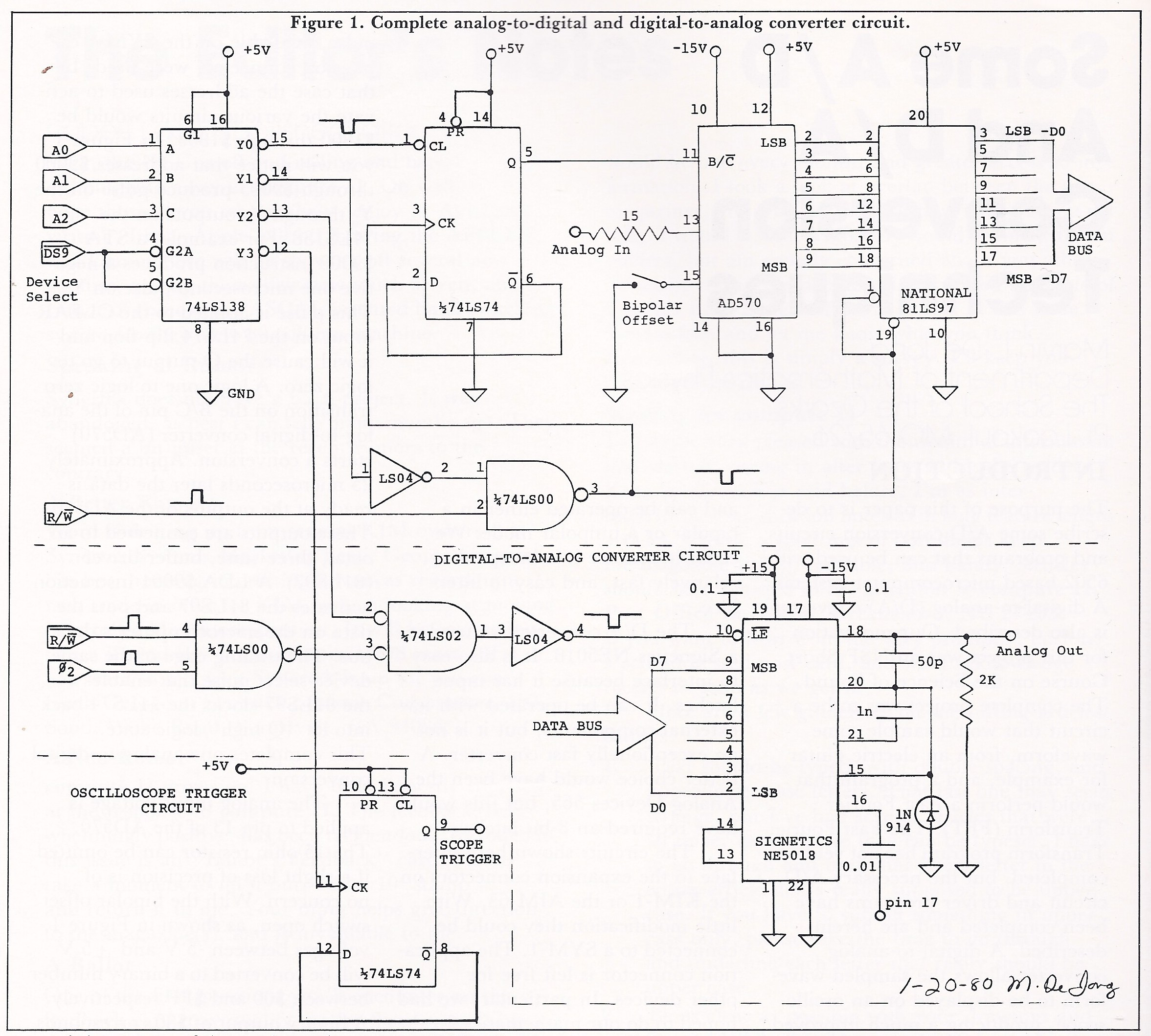
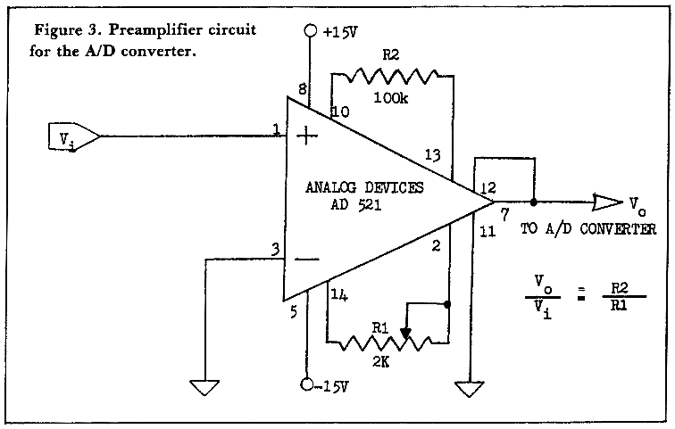
The analog input voltage is applied to pin 13 of the AD570. The 15 ohm resistor can be omitted if a slight loss of precision is of no concern. With the bipolar offset switch open, as shown in Figure 1, voltages between -5 V and +5 V will be converted to a binary number between $00 and $FF respectively. A binary output of $80 corresponds to pin 13 being at zero volts. If the bipolar output switch is closed, the AD570 will read voltages between 0 V and + 10 V. The AD 570 will also work with a negative supply voltage of -12 V rather than the -15 V shown in Figure 1. Although a “data ready” signal is available on the AD570, we chose to use software to wait for the conversion to be completed. One final note on the AD570: the input impedance for the analog input is only about 5 k ohm. Consequently it makes a very poor voltmeter unless a high impedance (a voltage follower circuit, for example) amplifier is placed between the analog input and the source of the analog voltage. We used the instrumentation amplifier (AD521) circuit given in Figure 3.
The digital-to-analog circuit is activated by a STA $9002 instruction. That is, to write to the NE5018, use a STA $9002 instruction and new data will be latched into the NE5018. The voltage at pin 18 is proportional to the 8-bit number written to the NE5018, shown operating in its bipolar mode in Figure 1
Finally, if you wish to use the A/D and D/A converters to implement a storage scope, then you may wish to use the other half of the 74LS74 flip-flop to produce a trigger signal. Two STA $9003 instructions produce a pulse on the Q output of the flip-flop that can be used as a trigger pulse to start the oscilloscope sweep.
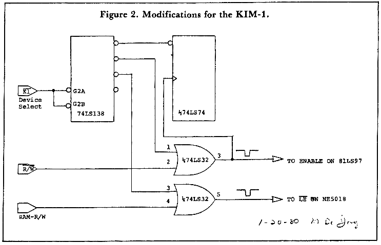
For all you purists who think that if it can't be done with a KIM-1 then it isn't worth doing, the circuit in Figure 1 will also work with a KIM-1. We simply replaced the DS9 device select with the Kl device select produced by the onboard 74145. A 3.3k pullup resistor is required. The entire circuit can be simplified somewhat with the modifications shown in Figure 2. The various 04s, 02s, and 00s are replaced with two gates on a 74LS32, the Kl device select goes to the 74LS138, and the remainder of the circuit is the same as in Figure 1. The RAM-RW signal on the KIM-1, which does not have the same meaning on the AIM 65, can be used to simplify the logic, as shown in Figure 2. The same simplification could probably be used with the SYM-1.
The preamplifier circuit we used to study several waveforms is shown in Figure 3. We used it as a gain of 100, and as a gain of 1000, amplifier, but it can also be operated at unity gain by adjusting Rl to be 100k. In this latter mode it simply provides a high impedance buffer for the AD570. The AD521 is a differential amplifier with a differential input impedance of about 3 × 10⁹ ohms. Pin 3, the - input, need not be grounded but can be connected directly to the input voltage source.
The circuits of Figures 1 - 3 provide a complete A/D and D/A system that can be used for a large variety of applications including voltage measurements, temperature measurements, and the storage scope application described here.
A/D and D/A Converter Software
The program in Example 1 was designed to work with the AIM 65 or any other system that has a 6522 VIA available for timing purposes. The addresses used to start the conversion, read the A/D converter, load the D/A converter, and trigger the oscilloscope are $9000 through $9003, respectively. If a device select other than the DS9 is used to enable the 74LS138 decoder, then these addresses must be changed accordingly. For example, if the DS18 select on the SYM-1 is used, then these addresses become $1800 through $1803, respectively. Since the KIM-1 does not have a 6522, we wrote another program that will work for it, and this program is listed in Example 2.
The program in Example 1 has a maximum sampling rate of one sample every 32 microseconds, or 31,250 Hz. It allows the AD570 exactly 28 microseconds to make a conversion if the T1 timer is loaded with $0000. If you have an AD570 that is slightly faster, try taking out the NOP instruction at $0F3A. If your AD570 is slightly slower, insert some extra NOP instructions after $0F3A. Change the various branch offsets accordingly. You can tell if you are giving the AD570 enough time by examining the data it returns.
The program in Example 1 has the following features. It continuously samples the analog voltage at the input of the A/D converter. When the conversion result exceeds a preassigned level stored in TRIG (location $0000), the program proceeds to sample another 255 points on the waveform at a rate determined by the numbers stored in TIMLO (location $0001) and TIMHI (location $0002). The 256 data points are stored in page two of memory. Once the data have been obtained, the program proceeds to read the data out, one point at a time, to the D/A converter for the purpose of displaying the values on an oscilloscope. Each time the 256 points are output to the D/A converter, a trigger pulse is also supplied. Since the conversion time is 32 microseconds with this program, there is no use loading the T1 timer with a number less than 32 unless you wish to sample at the maximum rate. In that case, put $00 in location $0001. In the program in Example 1, T1 is in its free running mode, so its interrupt flag, IFR6, will be set every N + 1 microseconds, where N is the 16-bit number loaded into T1 from locations $0001 and $0002. Be sure to load the locations TRIG, TIMLO, and TIMHI before running the program. The program comments should explain how the program works. The first two instructions may produce a dummy conversion, but their real function is to put the 74LS74 flip-flop in a condition with Q at logic one. The program consists of three main loops. The AGN loop continuously samples the incoming data, and the program branches out of this loop to the MORE loop when the incoming voltage exceeds the trigger level. In the MORE loop another 255 points are produced. When this data has been gathered, the program branches to the OUT loop to output the 256 points to the D/A converter.
Example 1. A/D and D/A driver program for 6522 based timing.
$0F00 8D 00 90  START   STA CVNST   Pulse 74LS74 flip-flop to be in a known
$0F03 AD 01 90          LDA A/D     condition with Q at logic one.
$0F06 A2 00             LDX $00     Initialize X register to zero
$0F08 A9 40             LDA $40     Initialize ACR of 6522 to put T1 in
$0F0A 8D 0B A0          STA ACR     its free-running mode.
$0F0D A9 00             LDA $00     Clear accumulator.
$0F0F F0 03             BEQ TEST    Branch to start the first conversion.
$0F11 AD 01 90  AGN     LDA A/D     Read A/D converter
$0F14 8D 00 90  TEST    STA CVNST   Start a conversion.
$0F17 8D 02 90          STA D/A     Output A/D to D/A converter.
$0F1A C5 00             CMP TRIG    Compare conversion result with trigger
$0F1C B0 0E             BCS SAMPLE  level. Branch to sample an additional
$0F1E A5 01             LDA TIMLO   255 points if A/D exceeds trigger level.
$0F20 8D 04 A0          STA T1LL    Load 6522 with the number of micro-
$0F23 A5 02             LDA TIMHI   seconds between conversions.
$0F25 8D 05 A0          STA T1LH    Start timer.
$0F28 90 37             BCC AGN     Branch to read A/D.
$0F2A AD 01 90  MORE    LDA A/D     Read A/D
$0F2D 8D 00 90  SAMPLE  STA CVNST   Start sampling waveform.
$0F30 9D 00 02          STA TAB,X   Previous result into table.
$0F33 E8                INX         X keeps track of the number of conversions.
$0F34 F0 0C             BEQ OUT     When X = 00, 256 conversions are complete.
$0F36 AD 04 A0          LDA T1CL    Clear T1 interrupt flag.
$0F39 EA                NOP         Fill in the 25 microsecond conversion
$0F3A EA                NOP         time with no operation instructions.
$0F3B 2C 0D A0  LOAF    BIT IFR     Has T1 timed-out?
$0F3E 70 E9             BVS MORE    Yes, get another conversion.
$0F40 50 F9             BVC LOAF    No, wait for timer.
$0F42 8D 03 90  OUT     STA SCPTRG  Trigger scope.
$0F45 EA                NOP         Use an eight microsecond pulse to
$0F46 EA                NOP         trigger scope.
$0F47 8D 03 90          STA SCPTRG
$0F4A BD 00 02  NEXPT   LDA TAB,X   Get some data from the table.
$0F4D 8D 02 90          STA D/A     Output it to the D/A and the scope.
$0F50 E8                INX
$0F51 D0 F7             BNE NEXPT   Branch to get more data.
$0F53 F0 ED             BEQ OUT

$0000 = TRIG   ; load with desired triggering level but not $00.
$0001 = TIMLO  ; low-order byte of time interval between samples (microseconds).
$0002 = TIMHI  ; high-order byte of time interval between samples.
$0200 = TAB    ; base address of table to store 256 samples.
$9000 = CNVST  ; a STA CVNST instruction will start an A/D conversion.
$9001 = A/D    ; the analog-to-digital converter is read at this location.
$9002 = D/A    ; write to this location to perform a digital-to-analog conversion.
$9003 = SCPTRG ; write to this location to trigger the oscilloscope.
The program in Example 2 works in about the same way with the same purpose in mind, but it was used on the KIM-1. The sampling rate with this program is once every 39 microseconds, or 25641 Hz. Its speed could be improved to be about the same as the program in Example 1. In any case, the on-board timers on the KIM-1 were used to produce the necessary timing. Again, the trigger level is stored in $0000, and the time is stored in $0001. The divide-by-one timer at $1704 on the KIM-1 was used, but the other timers may also be used.
Example 2. A/D and D/A driver program for a KIM-1 interface.
0300 8D 00 04  START   STA CVNST    Pulse 74LS74 flip-flop to be in a known
0303 AD 01 04          LDA A/D      condition with Q at logic one.
0306 A2 00             LDX $00      Initialize X register to zero.
0308 A9 00             LDA $00      Initialize accumulator to zero.
030A 8D 00 04  TEST    STA CVNST    Start A/D conversion.
030D 8D 02 04          STA D/A      Previous result into D/A converter.
0310 C5 00             CMP TRIG     Compare conversion result with trigger
0312 B0 16             BCS SAMPLE   level. Branch to sample 256 points if
0314 EA                NOP          voltage exceeds trigger level.
0315 EA                NOP          Delay with no-operation instructions
0316 EA                NOP          until the 25 microsecond conversion
0317 EA                NOP          time is completed.
0318 EA                NOP
0319 EA                NOP
031A EA                NOP
031B AD 01 04          LDA A/D      Read A/D converter.
031E 90 EA             BCC TEST     Branch to start another conversion.
0320 8D 00 04  MORE    STA CVNST    Start an A/D conversion.
0323 9D 00 02          STA TAB,X    Previous result into table.
0326 E8                INX          X keeps track of number of conversions.
0327 F0 13             BEQ OUT      When X = 00, 256 conversions are complete.
0329 A5 01     SAMPLE  LDA TIME     Get time in microseconds from $0001.
032B 8D 04 17          STA TIMER    Store in divide-by-one timer.
032E EA                NOP          Fill in time to make 25 microseconds
032F EA                NOP          before reading A/D converter.
0330 EA                NOP
0331 EA                NOP
0332 AD 01 04          LDA A/D      Read converter.
0335 2C 07 17  LOAF    BIT TIMER    Has timer timed out?
0338 30 E6             BMI MORE     Yes, then start another conversion and
033A 10 F9             BPL LOAF     store the result of the last. Otherwise
033C 8D 03 04  OUT     STA SCPTRG   wait. Trigger the oscilloscope.
033F A2 00             LDX $00
0341 8D 03 04          STA SCPTRG
0344 BD 00 02  NEXPT   LDA TAB,X    Get some data from the table.
0347 8D 02 04          STA D/A      Output it to the D/A and the oscillo-
034A E8                INX          scope.
034B D0 F7             BNE NEXPT    Branch to get more data.
034D F0 ED             BEQ OUT      Return to output table again.

$0000 = TRIG   ; load with desired triggering level.
$0001 = TIME   ; load with time (in microseconds) between samples.
$0400 = CVNST  ; a STA CVNST instruction will start an A/D conversion.
$0401 = A/D    ; the analog-to-digital converter is read at this location.
$0402 = D/A    ; write to this location to perform a digital-to-analog conversion.
$0403 = SCPTRG ; write to this location to trigger the oscilloscope.
The last program listing for the circuit in Figure 1 is a program that can be used to sample a waveform at as many points as your R/W memory will allow. Rather than use just one page of R/W memory for storing the waveform, it will use as many pages as you have available. The maximum sampling rate for this program is one sample every 43 microseconds or 23256 Hz. The program in Example 3 uses several of the same locations as the program in Example 1. The trigger level is stored in TRIG at $0000. The 16-bit number giving the number of microseconds between samples is stored in TIMLO at $0001 and TIMHI at $0002. The low-order byte of the base address of the table to store the conversion data is in location TAB at $0003. Normally this location initialized to $00. The high-order byte of the base address (page number) of the table is stored in TAB + 1 at $0004. For our experiments with the AIM 65 we used pages $02 through $0E. The page number of the last page you wish to fill with data is incremented by one and stored in location END at $0005. Thus if page $0E is the last page to be used to store data, then $0F is stored in END. Load location $0006, STARTP with the same value you put in $0004 if you wish to output all the results to the D/A for display on the oscilloscope.
The program in Example 3 samples an incoming waveform at N*256 points where N is the number of pages used to store the data. It then outputs all of these points to the D/A converter at the same rate that it sampled the waveform. If you want to output the results faster, replace the BIT IFR and BVC WAIT instructions at $0F5D with NOPs.
Example 3. N-Page A/D Conversion and Storage Program
$0F00 8D 00 90  START   STA CVNST   Pulse 7474 to be in a known condition,
$0F03 AD 01 90          LDA A/D     with Q at logic one.
$0F06 A0 00             LDY $00     Initialize Y to zero for indirect indexed
$0F08 A9 40             LDA $40     addressing that follows.
$0F0A 8D 0B A0          STA ACR     Put 6522 T1 in free-running mode.
$0F0D A9 00             LDA $00     Clear A.
$0F0F 8D 00 90  AGN     STA CVNST   Start a conversion.
$0F12 8D 02 90          STA D/A     Output result to D/A converter
$0F15 C5 00             CMP TRIG    Compare conversion result with trigger
$0F17 B0 21             BCS SAMPLE  level.
$0F19 A5 01             LDA TIMLO   Get low-order byte of time between conversions.
$0F1B 8D 04 A0          STA T1LL    Result into T1.
$0F1E A5 02             LDA TIMHI   Get high-order byte of time between
$0F20 8D 05 A0          STA T1LH    conversions
$0F23 AD 01 90          LDA A/D     Read A/D converter to get conversion level.
$0F26 90 E7             BCC AGN     Return to compare with trigger level.
$0F28 8D 00 90  DATA    STA CVNST   Start an A/D conversion.
$0F2B 91 03             STA (TAB),Y Result of previous conversion into table.
$0F2D C8                INY
$0F2E D0 0A             BNE EQUAL   Branch around the page number increment routine.
$0F30 E6 04             INC TAB + 1 Increment page number
$0F32 A5 04             LDA TAB + 1 Now compare it with the ending page
$0F34 C5 05             CMP END     number.
$0F36 90 09             BCC MORE    Fill another page.
$0F38 B0 14             BCS NOMORE  Table is filled, branch to output the table.
$0F3A EA        SAMPLE  NOP         These NOPs equalize the time between
$0F3B EA                NOP         loading the table when no page boundary
$0F3C EA                NOP         is crossed and when a page boundary is
$0F3D EA                NOP         crossed.
$0F3E EA                NOP
$0F3F A5 05             LDA TAB + 2 This is also a dummy instruction.
$0F41 AD 04 A0  MORE    LDA T1CL    Clear the T1 interrupt flag.
$0F44 AD 01 90          LDA A/D     Read the A/D converter.
$0F47 2C 0D A0  LOAF    BIT IFR     Has the timer timed-out?
$0F4A 70 DB             BVS DATA    Start another conversion.
$0F4C 50 F9             BVC LOAF    Wait for timer.
$0F4E 8D 03 90  NOMORE  STA SCPTRG  Trigger scope.
$0F51 A5 06             LDA STARTP  Reload TAB with starting page number.
$0F53 85 04             STA TAB + 1
$0F55 AD 04 A0  RPT     LDA T1CL    Clear T1 interrupt flag.
$0F58 B1 03             LDA (TAB),Y Get data from the table.
$0F5A 8D 02 90          STA D/A     Output it to D/A.
$0F5D 2C 0D A0  WAIT    BIT IFR     Test T1 flag.
$0F60 50 FB             BVC WAIT
$0F62 C8                INY
$0F63 D0 F0             BNE RPT     Get some more data for the D/A converter.
$0F65 E6 04             INC TAB + 1
$0F69 C5 05             CMP END
$0F6B 90 EA             BCC RPT     Get more data from a new page.
$0F6D B0 E1             BCS NOMORE  Output the table again.
We used this program to see how the waveform from a plucked guitar string varied with time, but we couldn't help connecting a microphone to the AD521 and using the program to output this speech sound to an audio amplifier. The results are quite good, even though we made no attempt to include low-pass filters in either the input or output circuits. The word spoken into the microphone and output to an audio amplifier is intelligible and one can easily identify the person who made the sound. We had enough storage capability on the AIM 65 to store one three-syllable word. If you want a project, you might try improving the circuit and program to do a better job with speech.
Results
In Figure 4 we show a photograph of the results of sampling a 1000 Hz sine wave at a rate of about 25,000 Hz. The photograph shows 256 points on the sine wave. Since we did not have a camera for our oscilloscope, the pictures were taken through a Celestron 5” telescope, placed about 25 ft. from the oscilloscope. Figure 5 shows the scope trace expanded to show just one cycle of the same waveform in Figure 4. Figure 6 shows 256 points of a 100 Hz sine wave sampled about once every 40 microseconds, while Figure 7 shows 256 points on a 10 Hz sine wave sampled once every 2000 microseconds. Figure 8 is the waveform of the A string of an electric guitar just after being plucked. The sampling rate in this case was about one sample every 85 microseconds. Finally, in Figure 9 we show a sampled version of a 2500 Hz sine wave. Clearly the system still does a pretty good job of reconstructing a 2500 Hz sine wave, but the information in frequencies much above 5000 Hz will be lost. Hopefully these pictures are worth a thousand words.
Figure 4. 256 points on a 1000 HZ Sine wave.
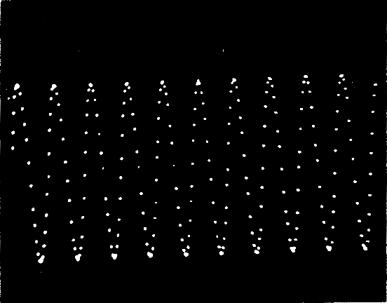
Figure 5. One cycle of a 1000 Hz Sine wave sampled at about 24,000 Hz.

Figure 6. 256 points on a 100 Hz Sine wave.
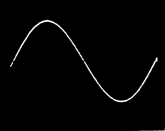
Figure 7. 256 points on a 10Hz Sine wave.
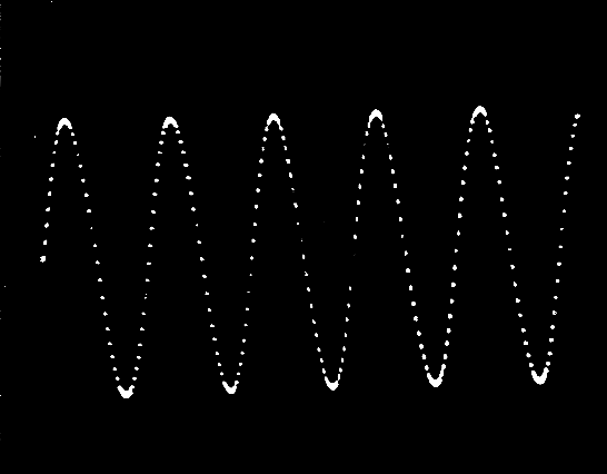
Figure 8. Plucked A string on an electric guitar.
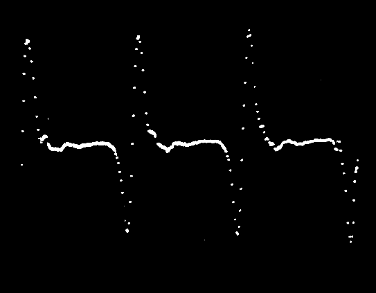
Figure 9. Several cycles of a 2500 Hz Sine wave.
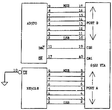
Figure 10. Interfacing the AD570 and the NE5018 to a 6522 Versatile Interface Adapter. Only data and control connection are shown in this figure. Refer to Figure 1 for the other details.
Appendix A. Interfacing The Converters To A 6522 VIA
The AD570 analog-to-digital converter and the NE5018 converter can easily be interfaced to a 6522, eliminating the need for most of the control logic shown in Figure 1. AIM 65 and SYM-1 users may wish to use the 6522 accessed at the application connector and the circuit shown in Figure 10. Note that only the data and control connections are shown in Figure 10. The other circuitry, mainly a few resistors and capacitors, can be found in Figure 1, as are the necessary power connections. This circuit eliminates the 74LS138, the 74LS74, the 81LS97, and the various NAND, NOR, and INVERTER chips. The CA2 pin on the 6522 could be used as an output to trigger the oscilloscope. Below find a short assembly language program that will collect 256 conversions and store them. This program has not been tried.
        LDA $FF     Set up Port A as an output port.
        STA DDRA
        LDA $18     Set up the ACR so the shift register shifts out (on CB2)
        ORA ACR     at the clock rata.
        STA ACR
        LDA $FE     Set up the PCR so a negative transition on CA1 sets
        AND PCR     its interrupt flag.
        STA PCR
HERE    LDA $03     The shift register is used to supply a 4 microsecond
        STA SR      pulse to the A/D converter to start a conversion.
        LDA $02     Test to see if conversion is complete by reading IFR1.
TEST    AND IFR
        BEQ TEST
        LDA IRB     Read the A/D converter.
        STA TAB,Y   Store the result in a one page table.
        INY
        BNE HERE    When Y = 0, 256 conversions are complete.
                    Otherwise get another conversion.
OUT