Here, in full, is Gene's Column 1. A portion of this column was printed in Issue 3 of COMPUTE. We thought we'd start at the beginning for Issue #1 of Compute II. RCL
Nuts and Volts
Gene Zunchak
Niagara Micro Design, Inc.
1700 Niagara Street
Buffalo, N.Y. 14207
With this article, I hope to begin a series of dissertations on the art and joy of doing it yourself. But first let me introduce myself. I'm Gene Zumchak. I graduated with an M.E.E. from Cornell in 1968. I paddled across Cayuga Lake and got my first job with a likable maverick named Robert Moog of Moog Synthesizer fame. I left my first, and one of the only legitimate jobs I've had in 1970. I moved to Buffalo and since that time have worked for a series of little flake outfits trying to find a winner, but at the same time, avoid having to work for a living. So far I've managed neither, but sure have had a lot of fun. But alas I think I'm getting closer. I now call myself Niagara Micro Design, Inc., and although the pay isn't that hot, the boss let's me play golf whenever the whim takes me (between thaws in July).
Anyway, I started drooling over micros in the early seventies when they first appeared in the electronic design magazines. Then in '75 an unknown semi company called MOS Technology made a big two month splash in the magazines (never to be heard from again) prior to a Western show. I clipped a coupon, sent in $25 and became the proud owner of a 40-legged centipede called a 6502. Now to give you some idea of just how fantastic that was, the 8080 chip set (8080, 8224, 8228) was selling for over $200. A few days after the chip arrived, I got a flyer advertising a single-board computer for just a few bucks more than the naked 8080 chip set. I ran to the bank, withdrew my life savings and sent in coupon number two becoming an even prouder owner of KIM-1 serial no. 00005. Soon afterwards, three friends and myself contracted to design and build five smart printer systems for Honeywell, without a TTY or assembler, let alone a development system. With little more than that KIM and a Simpson VOM we delivered five microprocessor controlled printers. Today, the same job would be a lot easier, but my “development system” is still just an expanded KIM. Anyone, in fact, can put together a development system for only a couple hundred dollars over the price of a KIM, SYM, AIM or other system. Putting together that development system is one of the topics I hope to get to in the future.
Presently I am working on a book entitled “Microcomputer Design and Maintenance” with the guidance of Jon Titus of the “Blacksburg Group” who hopefully will get it published. The topics presented in this series of articles in Compute will touch on some of the material in that book, as well as different material.
A dedicated micro system can be put together for under a $100. Why tie up your Apple or Pet to turn the furnace on, run your electric train, or program your wife's loom? Why not use your system as a tool to crank out dedicated controllers? I hope to show you how. Enough B.S. Let's start talking about hardware.
Read/Write Timing
The most important consideration in hardware design is read/write timing. It is not a complicated topic, but many “designers” avoid confronting it by surrounding a CPU with family chips (usually expensive) using circuits right out of the manuals. There's nothing wrong with the fancy family chips if you really need them. Oftentimes the most attractive chip may belong to another family. If you understand read/write timing, however, you may indeed be able to use a foreign chip.
Write Timing
The terms “reading” and “writing” always reflect the direction of data flow from the perspective of the processor. Thus in a “write” operation, data is presented by the processor to some external device, memory or output, and locked into that device. A bit of memory or output is a flip-flop. In memory, the output of the flip-flop can be read back into the processor. In “output”, the output of the flip-flop is connected to the world. (In some programmable devices, an output can often be read back into the processor.)
The usual type of flip-flop used with a processor is the “D type” flip-flop. A D flip-flop has a “D” or data input, and a clock (strobe) input which is an edge-sensitive function. That is, data is presented to the D input and is transferred to the output when the active edge occurs (usually positive going). An edge triggered flip-flop's output can change only on a clock edge. An example is the TTL 7474 dual D flip-flop. A variation of this is the transparent latch. It too has a D or data input, but a Gate input, instead of a strobe. When the gate is true, the output follows the data and is transparent to the data. Data is locked into the flip-flop on a false going gate edge. The 7475 is a quad transparent latch. In both types of flip-flops, data is locked in with a clock or gate edge.
In any latching operation, the following sequence occurs: Data is presented to an input, a locking edge occurs, and finally the data is removed. In general, the data to be written exists before and after the locking edge. We are now ready to define the important parameters of a write operation. The “setup” time is the minimum time the data must be present before the locking clock edge occurs. The “hold” time is how long the data must remain after the locking edge has gone away. The setup and hold times for a 7474 flip-flop are only 20 and 5 ns respectively. Since these times are so short, TTL latches can always be assured of working with MOS processors.
6502 Write Timing
A 6502 clock cycle is read cycle when the R/W line is high, and a write cycle when the R/W line is low. A cycle is divided into two (more or less) symmetrical halves. In the first half, the ø1 clock is high. The R/W line and the address lines change ø1. In ø2, data transfers occur. According to the spec sheet, the delay from the fall of ø2 to the beginning of the rise of ø1 can be zero (no max spec given). For zero delay, the ø1 clock is approximately ø2. However for external use, ø2 and ø2 are generally used. ø1 should not be used as a substitute for ø2. Figure 1. shows write timing for the 6502.
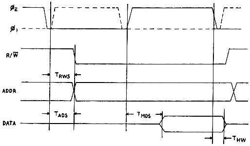
The R/W and address lines have a setup time (TRWS and TADS) as 300 ns maximum after the beginning of ø1. Data is available in a maximum of 200 ns after the rise of ø2 (TMDS). ø2 has a minimum width of 430 ns with a one micro second clock (1MHz). Thus data is available a minimum of 230 ns before the fall (locking edge) of the ø2 clock. The data is held beyond the fall of ø2 for a minimum of 30 ns (THW). Thus the 6502 is guaranteed to write successfully to any device with a setup time requirement of 230 ns or less, and a hold time requirement of 30ns or less. Implicit in the timing is that the falling edge of ø2 is the locking edge. The 6502 generates no write strobe. A write strobe must be fabricated by NANDing ø2 with the inverted R/W signal, R/W. This gives a strobe that goes low during ø2 only for a write cycle. In family devices, ø2 and R/W are applied separately and the gating is performed internally.
6502 Read Timing
In a read operation, an external device puts its data on the data lines and it is locked internally into the 6502 at the end of ø2. This timing is shown in figure 2.
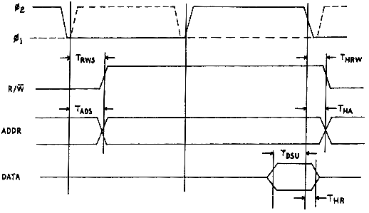
As in a write cycle, the address and R/W setup time is a maximum of 300 ns into ø1. The data setup time is a minimum 100 ns before ø2 (TDSU). In addition, the data must be held a minimum of 10 ns past ø2. Both the setup and hold times for the 6502 in a read operation are quite short making it easy to read I/O devices from any MOS family.
When a device is read, the data is gated onto the bus by a read gate generated from the R/W line and a decoded address. The strobing is done internally by the processor. A gating signal allows the data to overlap the strobe. It will be seen in many 6502 systems that read gates often incorporate ø2. It would appear that this would cut off the data at strobe time, and violate the hold time requirement. First of all, the tri-state gate buffering the data probably has a delay of at least 15 ns. Secondly, if ø2 has gone through one or two gates of buffering, it will occur 15 to 30 ns after the ø2 seen at the 6502. Thus the data will remain on the data bus 30 to 45 ns after ø2, even though ø2 appears to be used to cut data off.
Interfacing Non-family Devices
Meeting the read requirements of the 6502 is easy for almost any I/O device in any family. The problem occurs when the 6502 tries to write to the relatively sluggish devices of other families. Some of these chips have relatively long setup and hold time requirements for a write operation. The setup times are not often a problem, however. In order to be on the safe side, the chip manufacturer often quotes a rather conservative minimum hold time spec (like 100ns) while quoting a typical spec of 30 or even 0 ns. To insure reliable performance, you must meet the minimum spec. The 6502 will guarantee only a 30 ns write hold time. What do you do when you want to write to a Western Digital 1771 floppy controller chip with a longer hold time requirement? There are a number of ways to overcome this problem. First, however, we should consider an additional complication.
Earlier we saw that a little delay in the ø2 clock when used in a read gate was not a bad thing. However, delay in ø2 when used to generate a write strobe could be bad news. The 6502 provides for only 30 ns beyond the ø2 that it sees. A strobe generated from a delayed ø2 may in fact occur after the data has actually gone away. In this case, delay in the data path is beneficial. Any delay in ø2 greater than the delay in the data path takes away from the effective write hold time. Since few designers understand, let alone consider read/write timing, it is a wonder that most microcomputer systems work at all. In a typical single-board computer system, ø2 is generated on the board, buffered on some motherboard, and further buffered on the individual boards which plug into the motherboard. It is really questionable whether this buffering is really helpful. The fortunate thing for us all is that the hold time of the 6502 chips and the hold time requirement for I/O chips is almost always very conservatively speced.
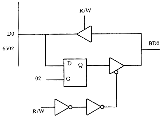
Let us consider some approaches for getting a little extra hold time. Figure 3. shows perhaps the safest way. The data bus write buffer consists of a transparent latch followed by a tri-state gate. The latch is gated with ø2 so that the data to be written is locked into the latch at the end of ø2. The R/W line ordinarily extends well into ø1 before changing. In fact the R/W line is not guaranteed to change for at least 300 ns (TRWS). To be on the safe side, we can always insert several gate delays in R/W so that the latched data will extend well beyond the end of ø2. This approach costs the addition of a pair of quad transparent latch chips, which may be very cheap insurance for reliable operation.
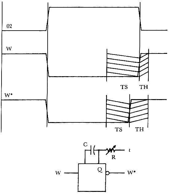
Another approach to getting a longer write hold time is to generate a write strobe which finishes earlier than ø2. This can be accomplished by hitting a one-shot with the regular write strobe. In this method, however, the longer hold time is at the expense of setup time. If you have lots of setup time to waste there's no problem. The width of the pulse will have to be adjusted carefully. Figure 4. shows the shortened write strobe, W* and setup time trade-off.
Access Time
When considering RAM or ROM, we need to consider access time, which is the time it takes the data to reach the output after the address is stable. For the 6502 at 1MHz, the addresses are good 300 ns into ø1. The data must be ready 100 ns before the end of ø2. This gives us about 600 ns of available access time. (The spec sheet guarantees 575.) If we could only steal another 75 ns, we could use much cheaper 650ns RAM and EPROM. If we pay a $5 premium for a 2MHz 6502, and run it at 1MHz, we can get an extra 150 ns from a shortened address setup time. The few extra dollars for the faster processor could save a lot more bucks on a system with lots of memory.
In summary, no serious, or at least no creative design can be undertaken without an understanding of read/write timing. It requires accommodating the setup and hold time requirements of the I/O devices with the corresponding times of the processor. Tricks like latching the write data can be used to overcome any discrepancies. The information is available from the device spec sheet.