Expanding KIM-Style 6502 Single Board Computers
Hal Chamberlin
Editor's Note: Hal ended his first installment with this . . .
The real question at this point then is: How many expansion boards can the unbuffered microprocessor bus drive before becoming overloaded? The 6502 microprocessor is rated to drive slightly more than 1 standard TTL load (equivalent to five low power shottky loads) on its address and data busses while most of the RAM's and ROM's tied to the data bus can drive two standard TTL loads. The 6520, 6522, and 6530 I/O chips have the same drive capability as the microprocessor. Thus in general the answer is at least four boards provided that the expansion boards themselves buffer the bus such that only one low power shottky load (.36MA in the zero state) is presented to the bus by the board. Many boards on the market and particularly those designed for an unbuffered bus do this. Actually, any well designed board would be expected to buffer the bus in order to provide clean signals for the remainder of the board logic. The reason that only four boards can be driven instead of five is that some of the address lines are loaded by a low power Shottky decoder IC on the computer board itself.
Part 2 of 3 The Great Experiment
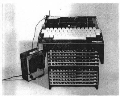
Of course loading the microprocessor with a full five loads puts the system right at the limit of rated drive current. One of the problems with testing digital circuitry is that there is no obvious indication of marginal operation that may later develop into a full fledged failure as components age. In order to determine the actual drive limit, the author took a fully stuffed AIM-65 (4K on-board RAM, assembler ROM and BASIC ROM's) and started adding Micro Technology K-1016 16K memory boards, the idea being to add boards until failure due to bus overload occurred. These boards use low power Shottky buffers onboard so each one would be expected to add a .36MA load to the bus.
Since the AIM's 40K of free addresses would only accomodate two of these boards, the most significant address bit was cut away from the bus at each socket position and instead connected to parallel output bits on the AIM's application connector. The boards were then jumpered to respond to addresses between 2000 and 5FFFF (hex). By programming only one output bit to be low at a time, a rudimentary bank switching setup was implemented. When the system was reset, all output bits automatically go high thus disabling all of the boards and preventing interference with the AIM monitor (since A15 was ignored, an enabled board would also respond to A000-DFFFF). A proper bank switch setup would have required a two-input OR gate (negative AND) to be tied to each of the A15 pins. In any case, it was adequate to run a memory test program.
The first trial was to install 4 of the 16K boards which worked fine as expected. Next, another card file was placed below the first and jumper wires added between the two motherboards. This gave a total of 9 bus slots which were filled with 16K memory boards. Again the memory test program (which wrote all 144K of memory with random data before reading any of it back) indicated no problem and the AIM monitor and BASIC continued to work flawlessly. A check with an oscilloscope revealed minimal signal degradation.
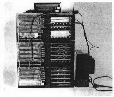
Finally, a third card file was added and bus jumpers installed to give a total of 14 slots. Three additional 16K memory boards were scrounged (I had no idea that more than 9 or 10 boards could be driven) to give a total of 192K of RAM. Again there were no obvious problems and the bus was being loaded to three times rated capacity! Figure 3 shows what the stack of card files looked like which is obviously impractical unless one cuts a hole in the tabletop to let the two extra card files hang below (I simply sat on a drafting stool to use the system). The rear view in figure 4 shows the interconnected motherboards and individual Board Enables from the application connector. Note the gridwork of copper braid between motherboards which makes the groundplane essentially continuous between the motherboards.
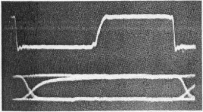
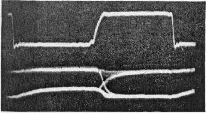
Photographs of the address and data bus signals were taken while running the memory test program and are shown in figure 5. About the only visible loading effect on the address bus is a long tail on the zero-to-one transition during phase 1 of the clock. The data bus appears to be even cleaner with just a shade over 100NS required for the data to stabilize after the leading edge of phase 2. The microprocessor was driving the data bus for the data bus for this photo (scope synced to read/write line on the bus). The zero logic levels, which one would think show the effect of gross overloading most, were still in the 0.3 volt range although the one levels were down to only 3 volts from a normal lightly loaded value of nearly 4 volts. Note the almost complete absence of noise. These "overloaded" signals actually look far better than most S-100 bus signals!
While these results are encouraging and certainly show that a four board load does not bring a system to the brink of failure, it does not mean that loading rules can be disregarded altogether. Some AIM's, as well as SYM's and KIM's, can be expected to have a weak component on-board that may not be able to drive a 12 board load adequately for reliable operation. Thus the "official" recommendation is to stick with the spec book and limit unbuffered systems to four boards. However, individual hobbyists should be able to go one or two boards over the limit with little probability of problems. Actually, addressing limitations are more likely to limit system size than bus drive capability with today's dense boards.