Double The Cassette Baud Rate Of Your OSI Superboard II/1P
Mr. James L. Mason Jacobus, Pennsylvania
I was thrilled when I received my Superboard II. It was my first micro, but being experienced in BASIC Programming (using a phone-linked ASR 33 with GE time-sharing) I had several programs which I was anxious to try. The Superboard performed perfectly. It did everything OSI said it would, however, 2 disadvantages of Superboard soon made themselves apparent. The 25 × 25 character video format was not the easiest to read. Secondly, the baud rate at which programs are saved and loaded from cassette seemed painfully slow. Having a good working background in digital electronics, I thought it might be possible to improve upon these two features. Upon close examination I found the video hardware was too intimate with the software in ROM. Fortunately, modifying the cassette port circuitry was a piece of cake and I was able to cut load and save time by half.
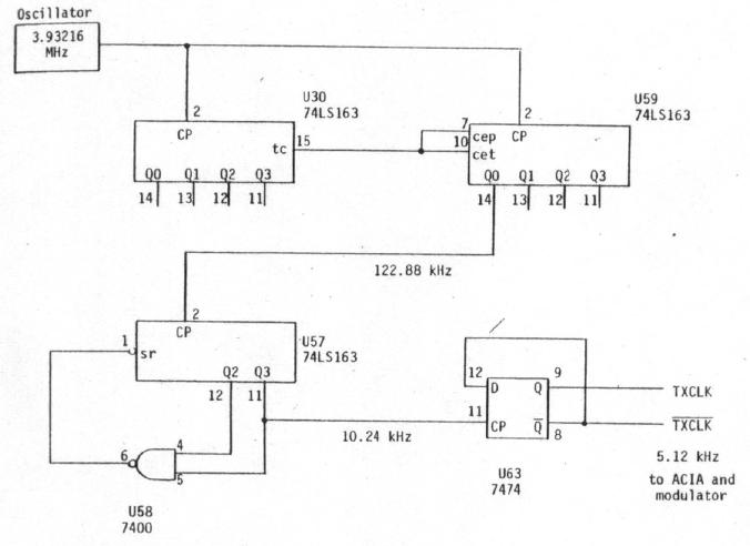
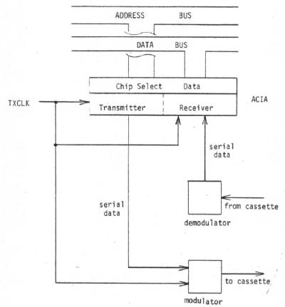
The cassette port utilizes a 6850 programable Asynchronous Communications Interface Adapter (see figure 1). When using this chip, the communications rate is determined by two things, the frequency of the clock which is applied to the TXCLK and RXCLK pins of the ACIA and the control word which is written into the ACIA's control register. I hypothesied that by doubling the clock frequency I could double the baud rate.
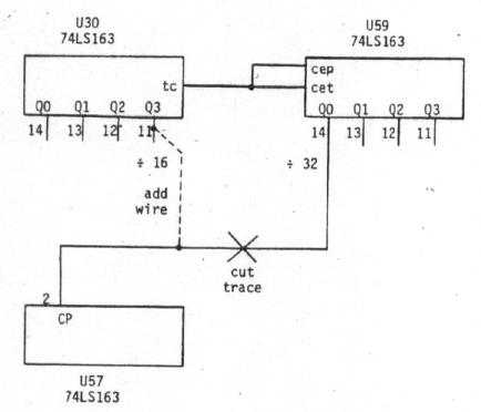
ON the Superboard, a crystal oscillator generates the base timing signal by which the entire board is controlled. This signal drives a synchronous divider chain (see figure 2). The timing signal destined for the ACIA comes off the ÷ 32 tap of this chain. The signal is finally divided by a ÷ 24 circuit composed of U57, U58, and U63. The resultant frequency of 5120 Hz is applied to the TXCLK input of the ACIA. The ACIA must be programmed to utilize a clock frequency either 64, 16, or 1 times the baud rate. The 320 baud rate is realized by programming the ACIA for a 16× clock rate.
To obtain a clock rate double of that which is used, I chose to sever the connection between U57 pin 2 and U59 pin 14 (see figure 3), then connect U57 pin 2 to U30 pin 11. I used a switch to maintain compatibility with my old 320 baud tapes.
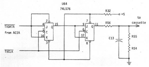
As far as the ACIA was concerned, the modification was done. However, there is one more block between the ACIA and the cassette machine, namely the Modulator/Demodulator.
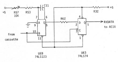
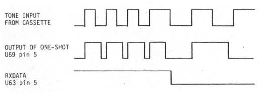
The modulator encodes the data in the form of tones. These tones are derived from the TXCLK (see Figure 4A). Since our new TXCLK is twice as fast, our tones will now be 2 times their original frequency. This poses no problem as far as modulation is concerned. It does, however, make a difference on the return trip. U69 determines what will be demodulated as a high or low tone (see figure 4B). A tone coming in will trigger the 74123 one-shot by it's rising edge (see figure 5). R57 is adjusted so that U69 will remain triggered until after the falling edge of the high frequency tone but not until the falling edge of a low frequency tone. The falling edge will clock the D flop U63 and propagate the state of U69. Because we now have shorter pulse widths, R57 must be adjusted to allow U69 to time-out during our new low tones. This was very simple to do. I simply saved a program using the new faster baud rate and attempted to load it back. While the program was trying to load, I adjusted R57 while watching the video monitor. I knew I had R57 adjusted properly when the program began appearing on the display, line by line. I experimented with R57 to find the points where data started to be garbled. The margin was surprisingly wide. Luckily, no software patch had to be made anywhere.
If you use a switch in your mod, remember you will have to readjust R57 each time you change baud rates. I see no reason why a DPDT switch couldn't be used to switch in a different resistor value for R57 along with switching the clock rate.