Experimenting With The 6551 ACIA
Marvin L. De Jong
Department of Mathematics-Physics
The School of the Ozarks
Pt. Lookout, MO
There is a growing interest in data communications, computer networks, time-sharing services and other forms of intercomputer communications. An important element in many data communications systems is an Asynchronous Communications Interface Adapter (ACIA). Both Rockwell International and Synertek manufacture a 6502 family device known as the 6551 ACIA. The purpose of this article is to provide information about interfacing this device to 6502-based microcomputers and to provide information about operating and controlling the 6551 with software.
Since I was not familiar with this chip, I decided to do some simple experiments with it to supplement the meager (in my opinion) information supplied by the specification sheets from Rockwell and Synertek. In particular, I decided to use my AIM 65 microcomputer as a smart terminal for a KIM-1, operating the latter in its "teletypewriter" mode. Although this may seem ridiculous, the idea might be useful in a laboratory where various student stations have a KIM-1 that is used for experiment control or data acquisition. If all the KIM-1s were connected to a central terminal, one could load a program into all of them simultaneously or, with the appropriate switching circuitry, one could collect and process data from each of them. In any case, the experiment taught me what a KIM-1 is like when operated in its TTY mode rather than from its keypad, and more importantly, I learned some things about the 6551 ACIA.
A circuit that can be used to interface the 6551 to a 6502-based microcomputer is shown in Figure 1. The connections to the microcomputer are on the left-hand side of the figure. The advantage of using a family-type chip is the ease with which the device may be interfaced to the microcomputer. Thus, the connections IRQ, RES, 02, R/W, and the data bus connections are all straightforward. If the lines between the microcomputer and the 6551 are kept short, a few inches or so, no buffering is required. This circuit was built on a protoboard attached to the expansion connector of an AIM 65. The four registers on the 6551 are selected with address lines A0 and A1 connected to the register select pins RS0 and RS1, respectively.
The chip select (or device select) signals, CS0 and
If you have a SYM-1 you can use device select
If you have a KIM-1 you can use one of the device selects K1 to K4 with suitable pull-up resistors, say 1000 ohms. Tie CS0 to + 5V.
If you have an APPLE II you can build the interface shown in Figure 1 on a peripheral card and plug it into one of the eight card slots. However, you must build your own decoding circuit because you cannot use either the device select (
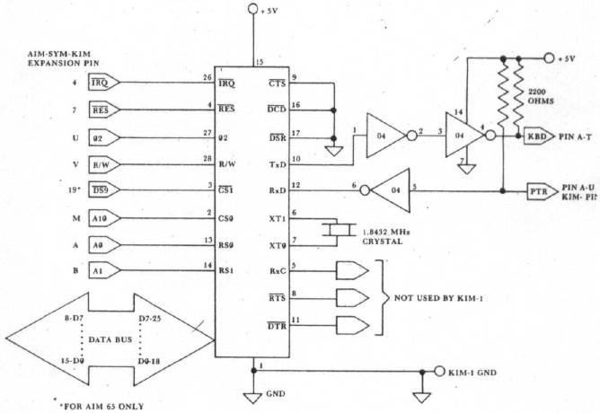
Proceeding to the circuitry on the right-hand side of Figure 1, you will note that you need a crystal whose frequency is 1.8432 MHz. The remaining connections are either input or output pins that connect the 6551 to devices outside of the microcomputer system, such as a modem or, in the experiment described here, another microcomputer. In this application only the data output (T×D) and data input (R×D) pins were used. A 74LS04 was used to provide suitable buffering between the 6551 and the KIM-1 printer and keyboard pins for the teletypewriter. The input pins
If A0 and A1 are used as register select signals, as indicated in Figure 1, then the low-order nibble of the address that accesses the 6551 will be $0, $1, $2, and $3 for the data registers, status register, command register, and control register, respectively. For example, if the address decoding scheme shown in Figure 1 is used, the transmitter data register is accessed by WRITING to $9400 and the receiver data register is accessed by READING location $9400. Writing to the status register at $9401 causes a pro�grammed RESET, and the status register is read at $9401. Refer to Figure 2 to identify the meaning of the bits in the status register.
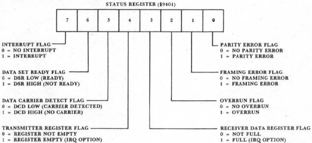
For the simple experiments described here the status register bits of most interest are the transmitter register flag and the receiver register flag. Writing to the transmitter register clears the register flag, and one should not write data to this register again until the data in the transmitter register has been transformed into a serial bit stream and has been transmitted by way of the T×D pin. When the word has been transmitted, bit four goes to logic one, and the transmitter data register is ready to accept another word. Likewise, when a complete word has been received by way of the R×D pin and the word is in the receiver data register, then bit three of the status register goes to logic one, and the word is ready to be read from the 6551. Both of the events just described may be used to produce interrupt requests (
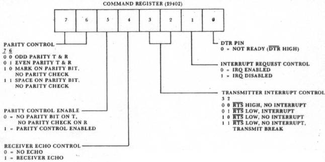
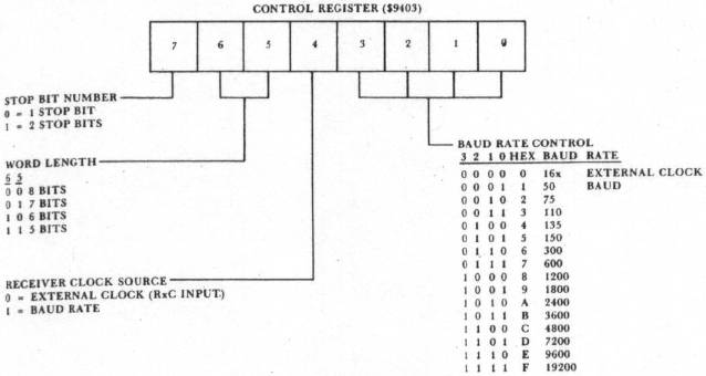
Refer to Figure 3 to identify the meaning of the various bits in the command register, and refer to Figure 4 to identify the meaning of the bits in the control register. The function of these registers will become apparent when we describe the program to uSe the AIM 65 as a terminal to control the KIM-1. In short, they allow the user to program the 6551 to operate under a large variety of conditions.
The program to test the 6551 with the AIM 65 and KIM-1 is given in Listing 1. The main program reads the keyboard and outputs this character to the 6551 transmit data register. The interrupt routine (remember to load the interrupt vectors if you use this program) reads the 6551 receive data register when the KIM-1 returns information to the AIM 65. In short, the entire program makes the AIM 65 behave exactly like a teletypewriter terminal as far as the KIM-1 is concerned. Since the 6551 is being operated in the interrupt mode, the first instruction in Listing 1 clears the 6502 interrupt flag to allow the 6551 to interrupt it. The next two instructions in the program load the command register. Refer to Figure 3 to see what bits were set or cleared. Since the KIM-1 software in the monitor simply strips the parity bit from any received word, the command register was initialized to disable and disregard any parity bits. Since the 6551 is being operated in an interrupt mode, bit one of the command register is cleared. However, it is the receiver portion of the 6551 that is being allowed to cause an interrupt, thus bit three of the command register is kept at logic one to prevent interrupts from the transmitter. The other bits of the command register control the handshaking signal pins of the 6551, and therefore they were not of any concern in this application.
The fourth and fifth instructions in Listing 1 load the control register. Refer to Figure 4. A "three" in the low-order nibble of the control register sets the Baud rate at 110. Higher Baud rates are possible, depending in part on whether the thermal printer on the AIM 65 is used. Without the printer operating, rates as high as 2400 Baud are possible. The usual teletypewriter data format is one start bit, seven data bits, one parity bit, and two stop bits. However, a number of formats will work, and we chose an eight bit word with one stop bit. Note however that the command register was set up for no parity bit, thus our word looks just like a word in the teletypewriter format. If we would have loaded the control register with $BA sending seven bits of word and two ?top bits at 2400 Baud, the program would still work. In order to interface the 6551 to any device you must program the command and control registers to match the protocol of the devices that are communicating.
Still keeping an eye on Listing 1, note that the next instruction is a subroutine jump to an AIM 65 subroutine that reads the keyboard and returns the ASCII code for the key depressed in the 6502 accumulator. This character is loaded into the 6551 transmit data register, and is promptly sent out on the T×D pin in serial form. Before getting another character, the program waits in a loop until the word is sent. It does this by examining bit four in the status register (refer to Figure 2). When the character has been sent and the transmit data register is empty, then the program loops back to get another character when the keyboard is scanned.
Refer next to the interrupt routine. A PHA instruction saves the accumulator. Next, the receive data register is read. The only time an interrupt occurs is when a new word is received from the KIM-1, and the second instruction of the interrupt routine gets the character in the accumulator of the AIM 65's 6502. Next, it outputs the character to the AIM 65 display. The fourth instruction clears the interrupt signal from the 6551. The accumulator is recalled, and the interrupt routine is concluded.
A future project includes interfacing the 6551 to a Novation Cat modem and trying to send information over telephone lines. Anyone out there care to join this experiment?
| Listing 1. Routines to Control the KIM-1 with an AIM 65. | |||
| CTRLRG = $9403; Control register of the 6551. | |||
| CMNDRG = $9402; Command register of the 6551. | |||
| STATUS = $9401; Status register of the 6551. | |||
| RDWR = $9400; Read/Write Data register of the 6551. | |||
| $0F00 58 | START | CLI | Clear interrupt flag. |
| 0F01 A9 09 | LDA #$09 | Set up command register. | |
| 0F03 8D 02 94 | STA CMNDRG | ||
| 0F06 A9 13 | LDA #$13 | Set up control register. | |
| 0F08 8D 03 94 | STA CTRLRG | Baud rate is 110. | |
| 0F0B 20 3C E9 REPEAT | JSR GETKEY | Get input character from the AIM 65 keyboard, output it to 6551. | |
| 0F0E 8D 00 94 | STA RDWR | ||
| 0F11 AD 01 94 | CHECK | LDA STATUS | Is transmit register empty? |
| 0F14 29 10 | AND #$10 | ||
| 0F16 F0 F9 | BEQ CHECK | No. Then wait here. | |
| 0F18 D0 F1 | BNE REPEAT | Yes. Then get another character. | |
| Interrupt Routine | |||
| $0E00 48 | IRQ | PHA | Save accumulator. |
| 0E01 AD 00 94 | LDA RDWR | Read the receive register and output the result. | |
| 0E04 20 7A E9 | JSR OUTCHAR | ||
| 0E07 AD 01 94 | LDA STATUS | Read the status register to clear the interrupt flag. | |
| 0E0A 68 | PLA | ||
| 0E0B 40 | RTI | Return to the main program. | |
| INTERRUPT VECTORS: [$A404] = $00; [$A405] = $0E |